Ordering information, Block diagram, Pin descriptions and equivalent circuits – Rainbow Electronics ADC08100 User Manual
Page 2
Ordering Information
ADC08100CIMT
TSSOP
ADC08100CIMTX
TSSOP (tape and reel)
ADC08100EVAL
Evaluation Board
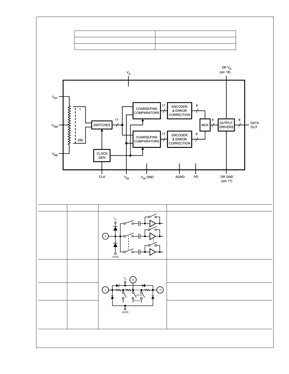
Block Diagram
10137102
Pin Descriptions and Equivalent Circuits
Pin No.
Symbol
Equivalent Circuit
Description
6
V
IN
Analog signal input. Conversion range is V
RB
to V
RT
.
3
V
RT
Analog Input that is the high (top) side of the reference
ladder of the ADC. Nominal range is 1.0V to V
A
. Voltage
on V
RT
and V
RB
inputs define the V
IN
conversion range.
Bypass well. See Section 2.0 for more information.
9
V
RM
Mid-point of the reference ladder. This pin should be
bypassed to a clean, quiet point in the analog ground
plane with a 0.1 µF capacitor.
10
V
RB
Analog Input that is the low side (bottom) of the
reference ladder of the ADC. Nominal range is 0.0V to
(V
RT
– 1.0V). Voltage on V
RT
and V
RB
inputs define the
V
IN
conversion range. Bypass well. See Section 2.0 for
more information.
ADC08100
www.national.com
2
- MAX5151 (16 pages)
- MAXQ3108 (64 pages)
- MAX5661 (39 pages)
- MAX6691 (7 pages)
- MAX5362 (12 pages)
- ADC10158 (26 pages)
- MAX8922L (14 pages)
- MAX8596Z (8 pages)
- MAX7491 (18 pages)
- MAX15040 (15 pages)
- MAX5177 (16 pages)
- ADC08138 (22 pages)
- MAX5961 (42 pages)
- T89C51RD2 (86 pages)
- MAX16055 (9 pages)
- MAX6659 (17 pages)
- ADC0820 (20 pages)
- MAX6678 (19 pages)
- MAX8884Z (15 pages)
- MAX16915 (9 pages)
- MAX8620 (18 pages)
- MAX5144 (12 pages)
- MAX6670 (8 pages)
- MAX8760 (39 pages)
- W78C32C (14 pages)
- MX7533 (8 pages)
- MAX8727 (13 pages)
- MAX9053 (15 pages)
- W78C54 (16 pages)
- MAX8614B (15 pages)
- W90N740 (219 pages)
- MAX6626 (13 pages)
- ADC10738 (30 pages)
- MAX17000 (31 pages)
- MAX5051 (21 pages)
- MAXQ1004 (18 pages)
- MAX6871 (51 pages)
- MX7847 (12 pages)
- MAX6608 (6 pages)
- MAX17083 (15 pages)
- MAX6641 (17 pages)
- MAX5251 (16 pages)
- MAX6338 (8 pages)
- MAX6690 (16 pages)
- MAX8668 (18 pages)