Pin descriptions – Rainbow Electronics DS1845 User Manual
Page 2
DS1845
2 of 13
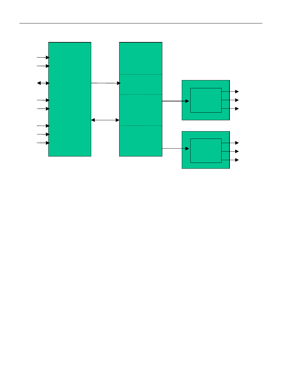
DS1845 BLOCK DIAGRAM Figure 1
Up to eight DS1845s can be installed on a single 2-wire bus. Access to an individual device is achieved
by using a device address that is determined by the logic levels of address pins A0 though A2.
Additionally, the DS1845 will operate from 3 volt or 5 volt supplies. Three package options are
available: Flip Chip Package, 16-ball STPBGA and 14-pin TSSOP.
PIN DESCRIPTIONS
V
CC
- Power Supply Terminal. The DS1845 will support supply voltages ranging from +2.7 to +5.5 volts.
GND - Ground Terminal.
SDA - 2-wire serial data interface. The serial data pin is for serial data transfer to and from the DS1845.
The pin is open drain and may be wire-ORed with other open drain or open collector interfaces.
SCL - 2-wire serial clock interface. The serial clock input is used to clock data into the DS1845 on rising
edges and clock data out on falling edges.
WP - Write Protect. Write Protect must be connected to GND before either the data in memory or
potentiometer wiper settings may be changed. Write Protect is pulled high internally and must be either
left open or connected to V
CC
if write protection is desired.
A0, A1, A2 - Address Inputs. These input pins specify the address of the device when used in a multi-
dropped configuration. Up to eight individual DS1845s may be addressed on a single 2-wire bus.
VCC
GND
SDA
SCL
WP
A0
A1
A2
H0
W0
L0
H1
W1
L1
248 BYTES
EEPROM
MEMORY
6 RESERVED
BYTES
1 BYTE WIPER
SETTING
POT 0
1 BYTE WIPER
SETTING
POT 1
CONTROL
DATA
POTENTIOMETER 0
2-WIRE
INTERFACE
POTENTIOMETER 1
100
Position
Pot
256
Position
Pot