Rainbow Electronics DS1845 User Manual
Page 11
DS1845
11 of 13
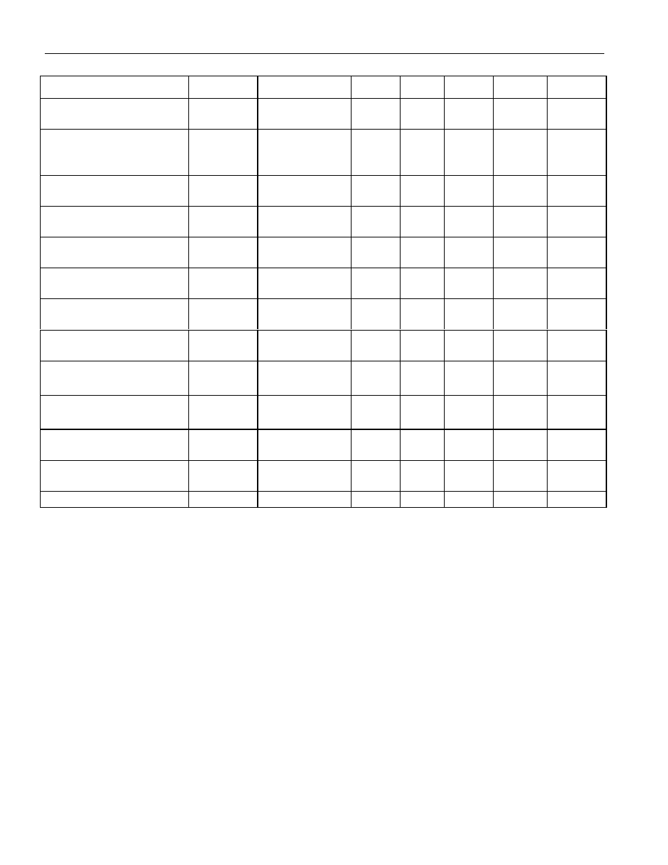
AC ELECTRICAL CHARACTERISTICS
(-40oC to 85oC, Vcc=2.7V to 5.5V)
PARAMETER
SYMBOL
CONDITION
MIN
TYP
MAX
UNITS
NOTES
SCL clock frequency
fSCL
0
0
400
100
kHz
*,6
**
Bus free time between
STOP and START
condition
tBUF
1.3
4.7
µ
s
*,6
**
Hold time (repeated)
START condition
tHD:STA
0.6
4.0
µ
s
*,7,6
**
Low period of SCL clock
tLOW
1.3
4.7
µ
s
*,6
**
High period of SCL clock
tHIGH
0.6
4.0
µ
s
*,6
**
Data hold time
tHD:DAT
0
0
0.9
µ
s
*,6,8
**
Data set-up time
tSU:DAT
100
250
ns
*,6
**
Start set-up time
tSU:STA
0.6
4.7
µ
s
*,6
**
Rise time of both SDA
and SCL signals
tR
20+0.1
CB
300
1000
ns
*,9
**
Fall time of both SDA
and SCL signals
tF
20+0.1
CB
300
300
ns
*,9
**
Set-up time for STOP
condition
tSU:STO
0.6
4.0
µ
s
*
**
Capacitive load for each
bus line
CB
400
pF
9
EEPROM write time
T
W
5
ms
10
* fast mode
** standard mode
NOTES
:
1. All voltages are referenced to ground.
2. I
STBY
specified with for V
CC
equal 3.0V and 5.0V and control port logic pins are driven to the
appropriate logic levels. Appropriate logic levels specify that logic inputs are within a 0.5V of
ground or V
CC
for the corresponding inactive state.
3. I/O pins of fast mode devices must not obstruct the SDA and SCL lines if V
CC
is switched off.
4. Address Inputs, A0, A1, and A2, should be tied to either V
CC
or GND depending on the desired
address selections.
5. I
STBY
specified with for V
CC
equal 3.0V and 5.0V and control port logic pins are driven to the
appropriate logic levels. Appropriate logic levels specify that logic inputs are within a 0.5V of
ground or V
CC
for the corresponding inactive state.