Ds4303 voltage sample and infinite hold, Detailed description, Pin description block diagram – Rainbow Electronics DS4303 User Manual
Page 6
DS4303
Voltage Sample and Infinite Hold
6
_____________________________________________________________________
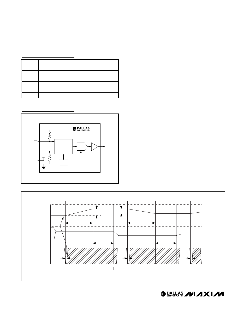
Detailed Description
The DS4303 provides a precise, NV output voltage,
V
OUT
, making it an ideal solution for factory calibration
of embedded systems. The DS4303 output voltage can
be adjusted over almost the entire operating supply
range of the device, and it can be precisely set to with-
in ±1mV. A graphical description of the DS4303 is pro-
vided in the block diagram.
During factory calibration, a simple adjustment proce-
dure must be followed. This entire procedure includes
setting V
IN
, toggling ADJ, waiting as V
OUT
self-adjusts,
and waiting for the completion of the EEPROM storage
cycle (See the timing diagram in Figure 1). At the start
of calibration, a voltage must be placed on V
IN
. This
voltage needs to be completely stable before the
adjustment procedure begins, and it must remain sta-
ble throughout the entire adjustment procedure. The
DS4303 will start its self-adjust procedure when the
ADJ pin is pulled low and held low for at least t
ADJ
,
after which it can be released at any time. Once ADJ
has been released, it should not be toggled again for
the remainder of the adjustment procedure. After the
falling edge on ADJ and the wait time, t
ADJ
, the V
OUT
self-adjust period begins. The length of the V
OUT
self-
adjust period can be determined using the formula
∆V x t
ST
, where
∆V is | V
OUT OLD
- V
OUT NEW
|.
ADJ
GND
V
OUT
V
CC
V
CC
V
IN
V
CC
R
PD
R
PU
V
REF
ADC
AND
CONTROL
EEPROM
12-BIT
DAC
DS4303
Figure 1. Timing Diagram
PIN
NAME
FUNCTION
1
ADJ
Adjust Control Input
2
GND
Ground
3
V
IN
Sample Voltage Input
4
V
OUT
Voltage Output
5
V
CC
Power-Supply Voltage
Pin Description
Block Diagram
V
OUT
V
IN
ADJ
t
W
t
W
FIRST PROGRAMMING CYCLE
ADDITIONAL PROGRAMMING CYCLES (IF REQUIRED)
t
ADJ
t
ADJ
t
ADJ
∆V
OUT
x t
ST
∆V
OUT
x t
ST
∆V
OUT
∆V
OUT