Detailed description, Pin descriptions – Rainbow Electronics DS1854 User Manual
Page 7
DS1854
Dual Temperature-Controlled Resistors with
Two Monitors
_____________________________________________________________________
7
Detailed Description
The user can read the registers that monitor the V
CC
,
MON1, MON2, and temperature analog signals. After
each signal conversion, a corresponding bit is set that
can be monitored to verify that a conversion has
occurred. The signals also have alarm flags that notify
the user when the signals go above or below the user-
defined value. Interrupts can also be set for each signal.
The position values of each resistor can be indepen-
dently programmed. The user can assign a unique
value to each resistor for every 2°C increment over the
-40°C to +102°C range. Both resistors can also be put
in a high-impedance mode using the RHIZ pin.
Two buffers are provided to convert logic-level inputs
into open-drain outputs. Typically these buffers are
used to implement transmit (Tx) fault and loss-of-signal
(LOS) alarms. Additionally, OUT1 can be asserted in
the event that one or more of the monitored values go
beyond user-defined limits.
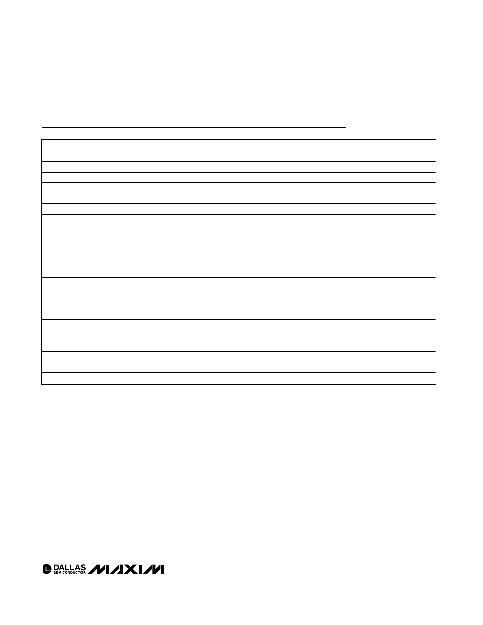
PIN
BALL
NAME
FUNCTION
1
B2
SDA
2-Wire Serial Data I/O pin. This pin is for serial data transfer to and from the device.
2
A2
SCL
2-Wire Serial Clock Input. The serial clock input is used to clock data into and out of the device.
3
C3
OUT1
Open-Drain Buffer Output
4
A1
IN1
TTL/CMOS-Compatible Input to Buffer
5
B1
OUT2
Open-Drain Buffer Output
6
C2
IN2
TTL/CMOS-Compatible Input to Buffer
7
C1
WPEN
Write Protect Enable. The device is not write protected if WPEN is connected to ground. This pin has
an internal pullup (R
WPEN
). See Table 6.
8
D1
GND
Ground
9
D3
RHIZ
Resistor Disable Input. When high, this signal places both resistors in an off-state or high-impedance
mode. When low, the resistors are on. This pin has an internal pullup (R
RHIZ
).
10
D4
MON1
External Analog Input
11
C4
MON2
External Analog Input
12
D2
L0
Low-End Resistor 0 Terminal. It is not required that the low-end terminals be connected to a potential
less than the high-end terminals of the corresponding resistor. Voltage applied to any of the resistor
terminals cannot exceed the power-supply voltage, V
CC
, or go below ground.
13
B3
H0
High-End Resistor 0 Terminal. It is not required that the high-end terminals be connected to a
potential greater than the low-end terminals of the corresponding resistor. Voltage applied to any of
the resistor terminals cannot exceed the power-supply voltage, V
CC
, or go below ground.
14
B4
L1
Low-End Resistor 1 Terminal
15
A4
H1
High-End Resistor 1 Terminal
16
A3
V
CC
Supply Voltage
Pin Descriptions