Rainbow Electronics aP89085 User Manual
Page 13

Integrated Circuits Inc.
aP89341/170/085
Ver 2.1 12 Aug 24, 2006
1. Signal output from the pin, OUT2, is defined by G[3:0], as below:
G[3:0]
OUT2
G[3:0]
OUT2
000
BUSYB
100
1KHz
001
8KHz
101
16Hz
010
4KHz
110
1MHz
011
2KHz
111
FULLB
2. If the STATUS is not executed, default value of OUT2 is the internal Reset signal.
3. BUSYB is the logical inversion of BUSY.
4. EMPTY (or FULLB) is the logical inversion of FULL.
5. Only the 1MHz clock will not be stopped by the PAUSE command.
•
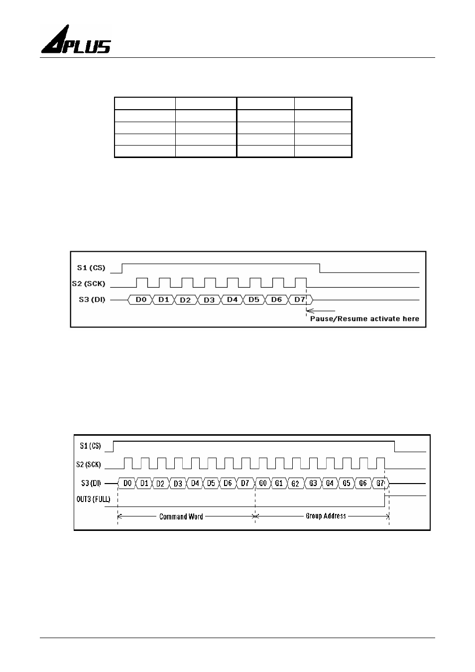
Pause and Resume (PLAUS-39H; RESUME-1DH)
Fig. 15 Pause and Resume command timing
6. In Pause state, VOUT1 and VOUT2 will stay at logic LOW while the COUT will stay at
the current D/A data level (i.e. COUT is kept outputting an DC current). When Resume,
the COUT data will continue at the current D/A data level.
7. The Pause state will be released by PDN1, PDN2, PLAY and RESUME commands.
•
Prefetch Voice Group Address (PREFETCH-71H)
Fig. 16 Prefetch next Voice Group timing
1. The PREFETCH command pre-load the next Voice Group Address into the address buffer.
2. The OUT3 output (FULL) will become logic HIHG once the Group Address is successfully
loaded.
3. The Voice Group will be played once the playing of the current Voice Group is finished.
4. The FULL signal will become logic LOW once the Voice Group is played and the address
buffer is released and ready for next PREFECT action.
5. Using the PREFECT make sure there is no gap between each Voice Group.
