High-voltage serial programming characteristics, Low-voltage serial downloading, Figure 34 – Rainbow Electronics AT90LS2343 User Manual
Page 42: Table 17
42
AT90S/LS2323/2343
1004D–09/01
High-voltage Serial Programming Characteristics
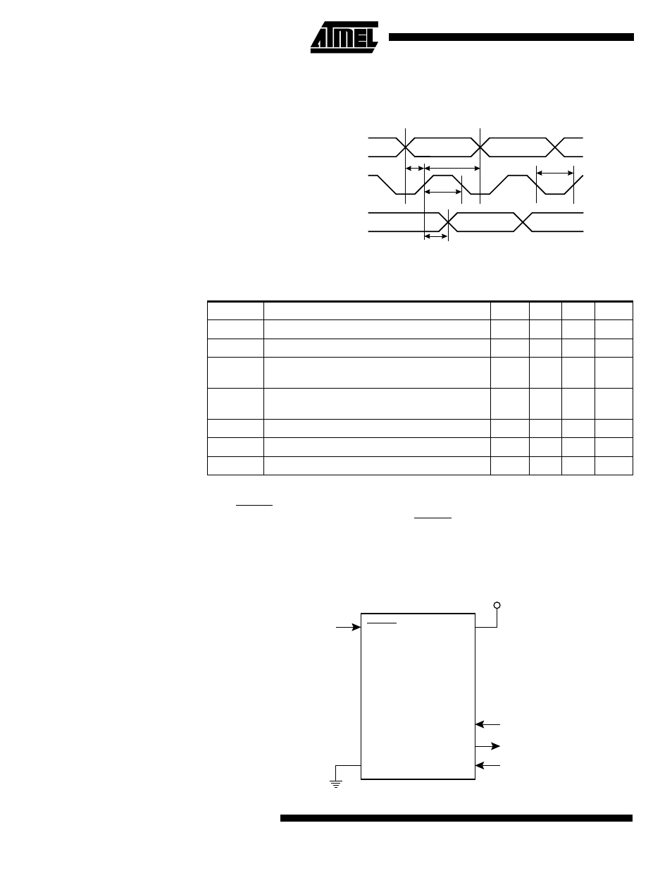
Figure 34. High-voltage Serial Programming Timing
Low-voltage Serial
Downloading
Both the program and data memory arrays can be programmed using the serial SPI bus
while RESET is pulled to GND. The serial interface consists of pins SCK, MOSI (input)
and MISO (output) (see Figure 35). After RESET is set low, the Programming Enable
instruction needs to be executed first before program/erase instructions can be
executed.
Figure 35. Low-voltage Serial Programming and Verify
Table 17. High-voltage Serial Programming Characteristics, T
A
= 25
°C ± 10%, V
CC
=
5.0V ± 10% (unless otherwise noted)
Symbol
Parameter
Min
Typ
Max
Units
t
SHSL
SCI (XTAL1/PB3) Pulse Width High
100.0
ns
t
SLSH
SCI (XTAL1/PB3) Pulse Width Low
100.0
ns
t
IVSH
SDI (PB0), SII (PB1) Valid to SCI (XTAL1/PB3)
High
50.0
ns
t
SHIX
SDI (PB0), SII (PB1) Hold after SCI (XTAL1/PB3)
High
50.0
ns
t
SHOV
SCI (XTAL1/PB3) High to SDO (PB2) Valid
10.0
16.0
32.0
ns
t
WLWH_CE
Wait after Instr.3 for Chip Erase
5.0
10.0
15.0
ms
t
WLWH_PFB
Wait after Instr.3 for Write Fuse Bits
1.0
1.5
1.8
ms
SDI (PB0), SII (PB1)
SDO (PB2)
SCI (XTAL1/PB3)
t
IVSH
t
SHSL
t
SLSH
t
SHIX
t
SHOV
RESET
GND
VCC
PB2
PB1
PB0
SCK
MISO
MOSI
2.7 - 6.0V
AT90S/LS2323,
AT90S/LS2343
GND