Ds4412 dual-channel, i, C adjustable sink/source current dac, Application information – Rainbow Electronics DS4412 User Manual
Page 9: Package information
DS4412
Dual-Channel, I
2
C Adjustable
Sink/Source Current DAC
Maxim cannot assume responsibility for use of any circuitry other than circuitry entirely embodied in a Maxim product. No circuit patent licenses are
implied. Maxim reserves the right to change the circuitry and specifications without notice at any time.
Maxim Integrated Products, 120 San Gabriel Drive, Sunnyvale, CA 94086 408-737-7600 _____________________ 9
© 2007 Maxim Integrated Products
is a registered trademark of Maxim Integrated Products, Inc.
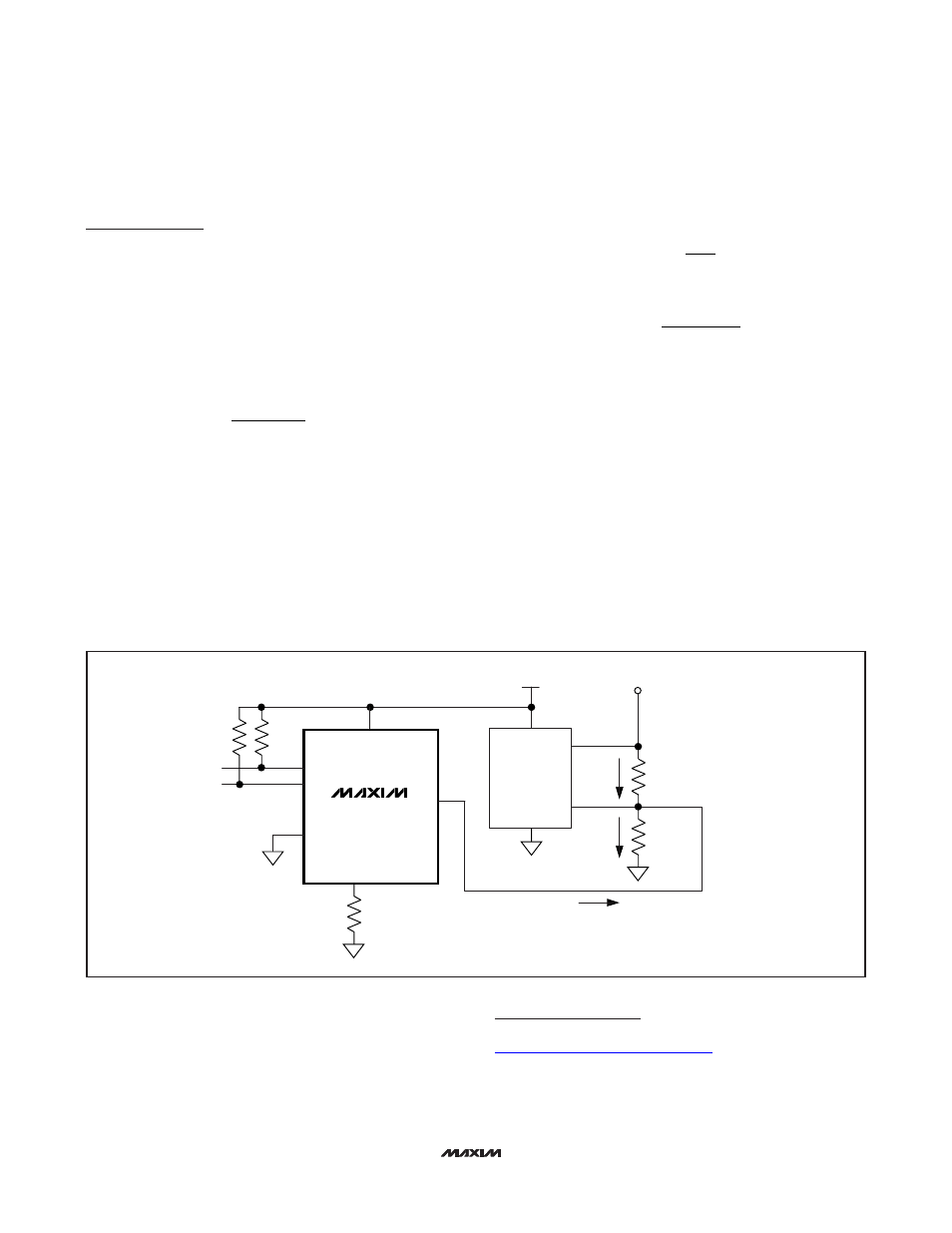
Application Information
Example Calculation
for an Adjustable Power Supply
In this example, the Typical Operating Circuit is used
as a base to create Figure 3, a 2.0V voltage supply with
±20% margin. The adjustable power supply has a
DC-DC converter output voltage, V
OUT
, of 2.0V and a
DC-DC converter feedback voltage, V
FB
, of 0.8V. To
determine the relationship of R
0A
and R
0B
, we start with
the equation:
Substituting V
FB
= 0.8V and V
OUT
= 2.0V, the relation-
ship between R
0A
and R
0B
is determined to be:
R
0A
= 1.5 x R
0B
I
OUT0
is chosen to be 1mA (midrange source/sink cur-
rent for the DS4412). Summing the currents into the
feedback node, we have the following
Where:
And
To create a 20% margin in the supply voltage, the value
of V
OUT
is set to 2.4V. With these values in place, R
0B
is
calculated to be 267
Ω, and R
0A
is calculated to be 400
Ω.
The current DAC in this configuration allows the output
voltage to be moved linearly from 1.6V to 2.4V using 15
settings. This corresponds to a resolution of 25.8mV/step.
V
CC
Decoupling
To achieve the best results when using the DS4412,
decouple the power supply with a 0.01µF or 0.1µF
capacitor. Use a high-quality ceramic surface-mount
capacitor if possible. Surface-mount components mini-
mize lead inductance, which improves performance,
and ceramic capacitors tend to have adequate high-
frequency response for decoupling applications.
I
V
V
R
R A
OUT
FB
A
0
0
=
−
I
V
R
R B
FB
B
0
0
=
I
I
I
OUT
R B
R A
0
0
0
=
−
V
R
R
R
V
FB
B
A
B
OUT
=
+
×
0
0
0
DC-DC
CONVERTER
FB
OUT
SDA
SCL
OUT0
GND
R
FS0
= 4.612k
Ω
4.7k
Ω
4.7k
Ω
V
CC
V
CC
V
OUT
= 2.0V
FS0
R
0B
= 267
Ω
R
0A
= 400
Ω
V
FB
= 0.8V
I
R0A
I
R0B
I
OUT0
DS4412
Figure 3. Example Application Circuit
Package Information
For the latest package outline information, go to
www.maxim-ic.com/DallasPackInfo
.