Apr9600, Integrated circuits inc, Bonding pad diagram and bonding pad coordinates – Rainbow Electronics APR9600 User Manual
Page 15
INTEGRATED CIRCUITS INC.
-
APR9600
http://www.aplusinc.com.tw
Page / 17 Ver2.1
15
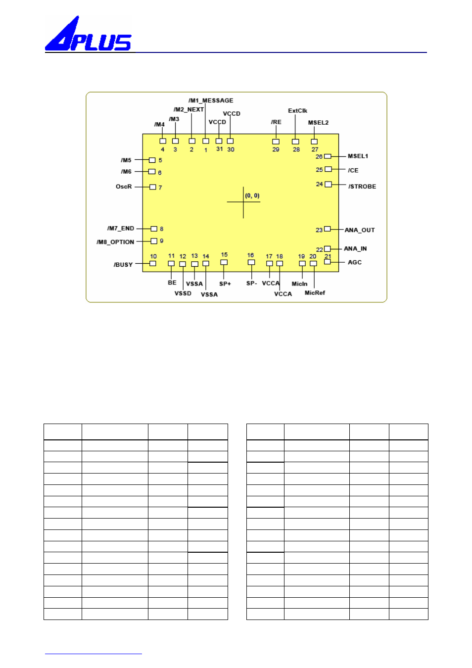
5. Bonding Pad Diagram and Bonding Pad Coordinates :
Figure 6 APR9600 Die Bonding Pad Diagram
Notes:
Die Dimensions
X-Axis: 212 +/- 1 mils
(X-Axis: 5450 um)
Y-Axis: 176 +/- 1 mils
(Y-Axis: 4550 um)
Die Thickness
13.8 +/- 1.0 mils
(350 +/- 25 um)
Pad Opening
4.3 mils
(110 um)
Table 7 Bonding Pad Coordinates For The APR9600 Device.
Pad No. Pad Name
X Axis Y Axis
Pad No.
Pad Name
X Axis Y Axis
1 /M1_MESSAGE
-1075
2007
17 VCCA 844
-1909
2 /M2_NEXT
-1393
2007
18 VCCA 1066
-1951
3 /M3
-1833
2007
19 MicIn 1708
-1969
4 /M4
-2151
2007
20 MicRef 2064
-1969
5
/M5
-2513 1397
21
AGC
2491 -1865
6
/M6
-2513 1079
22
ANA_IN
2491 -1513
7
OscR
-2513 617
23
ANA_OUT
2491 -1013
8
/M7_END
-2485 -865
24
/STROBE
2514 696
9
/M8_OPTION
-2485 -1193
25
/CE
2514 1182
10
/BUSY
-2435 -1987
26
MSEL1
2514 1532
11
BE
-1953 -1987
27
MSEL2
2121 2007
12
VSSD
-1728 -2003
28
ExtClk
1592 2007
13
VSSA
-1532 -1976
29
/RE
1088 2007
14
VSSA
-1337 -1952
30
VCCD
-577 2007
15
SP+
-840 -1838
31
VCCD
-757 2007
16
SP-
347 -1838
Note: All coordinates are with respect to the center of the die (um)