Apr9600, Integrated circuits inc, Electrical characteristics – Rainbow Electronics APR9600 User Manual
Page 14
INTEGRATED CIRCUITS INC.
-
APR9600
http://www.aplusinc.com.tw
Page / 17 Ver2.1
14
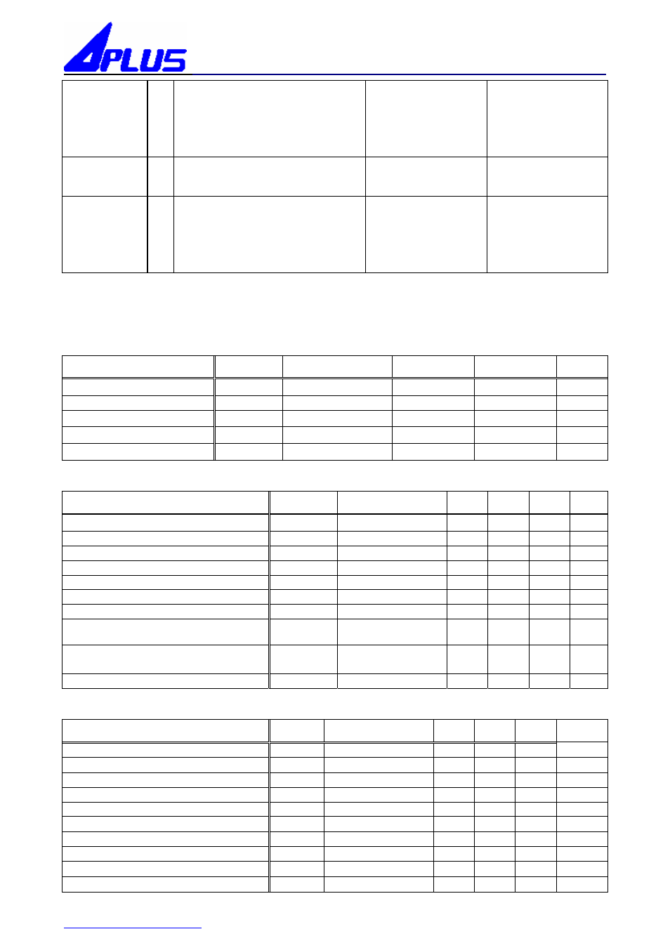
ExtClk 26
External Clock: This clock can be
used instead of the internal clock
for greater programming control
and or accuracy. When using the
internal clock this pin should be tied
to system GND.
Same as Random
Access Mode.
Same as Random
Access Mode.
/ RE
27
Record Enable: this pin controls
whether the device is in write or
read mode. Logic level high is read.
Same as Random
Access Mode.
Same as Random
Access Mode.
VCCD 28
Digital Positive Power Supply: This
connection supplies power for
on-chip digital circuitry. Should be
connected to the positive supply
rail as outlined in the reference
schematics.
Same as Random
Access Mode.
Same as Random
Access Mode.
4. Electrical Characteristics :
The following tables list absolute maximum ratings, DC Characteristics, and Analog
Characteristics for the APR9600 device.
Table 4 Absolute Maximum Ratings
Item
Symbol
Condition
Min
Max
Unit
Power Supply voltage
VCC
TA = 25℃
-0.3 7.0
V
Input Voltage
VIN
IIN<20mA
-1.0
Vcc + 1.0
V
Storage Temperature
TSTG
-
-65
150
℃
Temperature Under Bias
TBS
-
-65
125
℃
Lead Temperature
TLD
<10s
-0.3
300
℃
Table 5 DC Characteristics
Item Symbol
Condition
Min
Typ
Max Unit
Power Supply voltage
VCC
TA = 25℃
4.5 - 6.5
V
Input High Voltage
VIN -
2.0 - V
Input Low Voltage
VIL - -
-
0.8 V
Output High Voltage
VOH
IOH=-1.6mA
2.4 - - V
Output Low Voltage
VOL
IOL=+4.0mA
-
-
0.45
V
Input Leakage Current
VIH=Vcc
-
-
-
1.0
uA
Input Leakage Current
IIL
VIL=Vss
-1.0
uA
Output Tri-state Leakage Current
IOZ
VOUT=Vcc or
VOUT=VSS
-1.0 1.0
uA
Operating Current Consumption
ICC
Internal Clock No
Load
- 25 - mA
Standby Current Consumption
ICCS
No Load
-
1.0
-
uA
Table 6 Analog Characteristics*
Item Symbol
Condition
Min
Typ
Max
Unit
Micln Input Voltage
VMI
30
mVP-P
Micln Input Resistance
RMI
15
kΩ
Micln Amp Gain (1)
GMI1
AGC=2.25V
30
dB
Micln Amp Gain (2)
GM2
AGC=3.8V
-2
dB
ANA_IN Input Voltage
VANI
140
mVP-P
ANA_IN Input Resistance
RANI
500
kΩ
ANA_IN Amp Gain
GANI
ANA_IN to SP+/-
10
dB
AGC Output Resistance
RAGC
225
KΩ
Sp+/- Output Power
PSP
RSP+/-=16Ω
12.2
MW
Voltage Amplitude across SP+/-
VSP
RSP+/-≧16Ω
1.4
VP-P