Transfer characteristics, Figure 1. transfer characteristics, Note 4) – Rainbow Electronics ADC12281 User Manual
Page 7: Note 5), Note 6), Note 10), Note 11), Note 14), Ac electrical characteristics
AC Electrical Characteristics
(Continued)
Note 4: The absolute maximum junction temperature (T
JMAX
) for this device is 150˚C. The maximum allowable power dissipation is dictated by T
JMAX
, the
junction-to-ambient thermal resistance (
θ
JA
), and the ambient temperature (T
A
), and can be calculated using the formula P
D
MAX = (T
JMAX
– T
A
) /
θ
JA
. In the 32-pin
TQFP,
θ
JA
is 79˚C/W, so P
D
MAX = 1,582 mW at 25˚C and 949 mW at the maximum operating ambient temperature of 75˚C. Note that the power dissipation of this
device under normal operation will typically be about 125 mW (typical power dissipation + 20 mW TTL output loading). The values for maximum power dissipation
listed above will be reached only when the ADC12281 is operated in a severe fault condition (e.g., when input or output pins are driven beyond the power supply
voltages, or the power supply polarity is reversed). Obviously, such conditions should always be avoided.
Note 5: Human body model is 100 pF capacitor discharged through a 1.5 k
Ω resistor. Machine model is 220 pF discharged through 0Ω.
Note 6: See AN-450, “Surface Mounting Methods and Their Effect on Product Reliability”, or the section entitled “Surface Mount” found in any post 1986 National
Semiconductor Linear Data Book, for other methods of soldering surface mount devices.
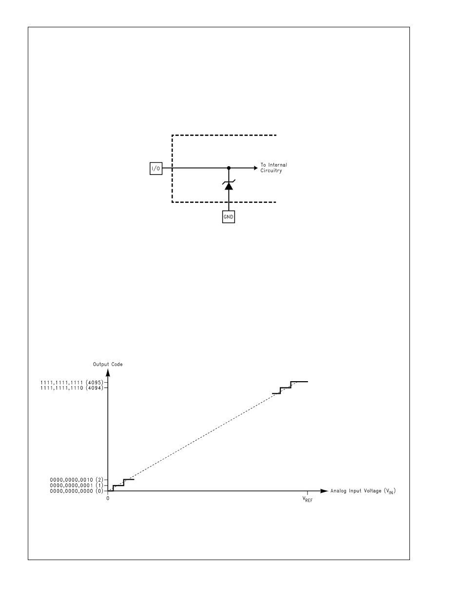
Note 7: The inputs are protected as shown below. Input voltage magnitudes up to 5V above V
A
or to 5V below GND will not damage this device, provided current
is limited per (Note 3). However, errors in the A/D conversion can occur if the input goes above V
A
or below GND by more than 100 mV. As an example, if V
A
is 4.75V,
the full-scale input voltage must be
≤ 4.85V to ensure accurate conversions.
10102708
ESD Protection Scheme for Analog Input and Digital Output Pins
Note 8: To guarantee accuracy, it is required that |V
A
–V
D
|
≤ 100 mV and separate bypass capacitors are used at each power supply pin.
Note 9: With the test condition for V
REF
= +2.0V, the 12-bit LSB is 488 µV.
Note 10: Typical figures are at T
A
= T
J
= 25˚C, and represent most likely parametric norms. Test limits are guaranteed to National’s AOQL (Average Outgoing
Quality Level).
Note 11: Tested limits are guaranteed to National’s AOQL (Average Outgoing Quality Level).
Note 12: Integral Non-Linearity is defined as the deviation of the analog value, expressed in LSBs, from the straight line that passes through positive full-scale and
zero.
Note 13: Timing specifications are tested at the TTL logic levels, V
IL
−0.4V for a falling edge and V
IH
= 2.4V for a rising edge. TRI-STATE output voltage is forced
to 1.4V.
Note 14: Optimum SNR performance will be obtained by keeping the reference input in the 1.8V to 2.2V range. The LM4041CIM3-ADJ (SOT-23 package), the
LM4041CIZ-ADJ (TO-92 package), or the LM4041CIM-ADJ (SO-8 package) bandgap voltage reference is recommended for this application.
Transfer Characteristics
10102709
FIGURE 1. Transfer Characteristics
ADC12281
www.national.com
7