Figure 5. suggested application circuit, 0 digital inputs, Applications information – Rainbow Electronics ADC12281 User Manual
Page 13
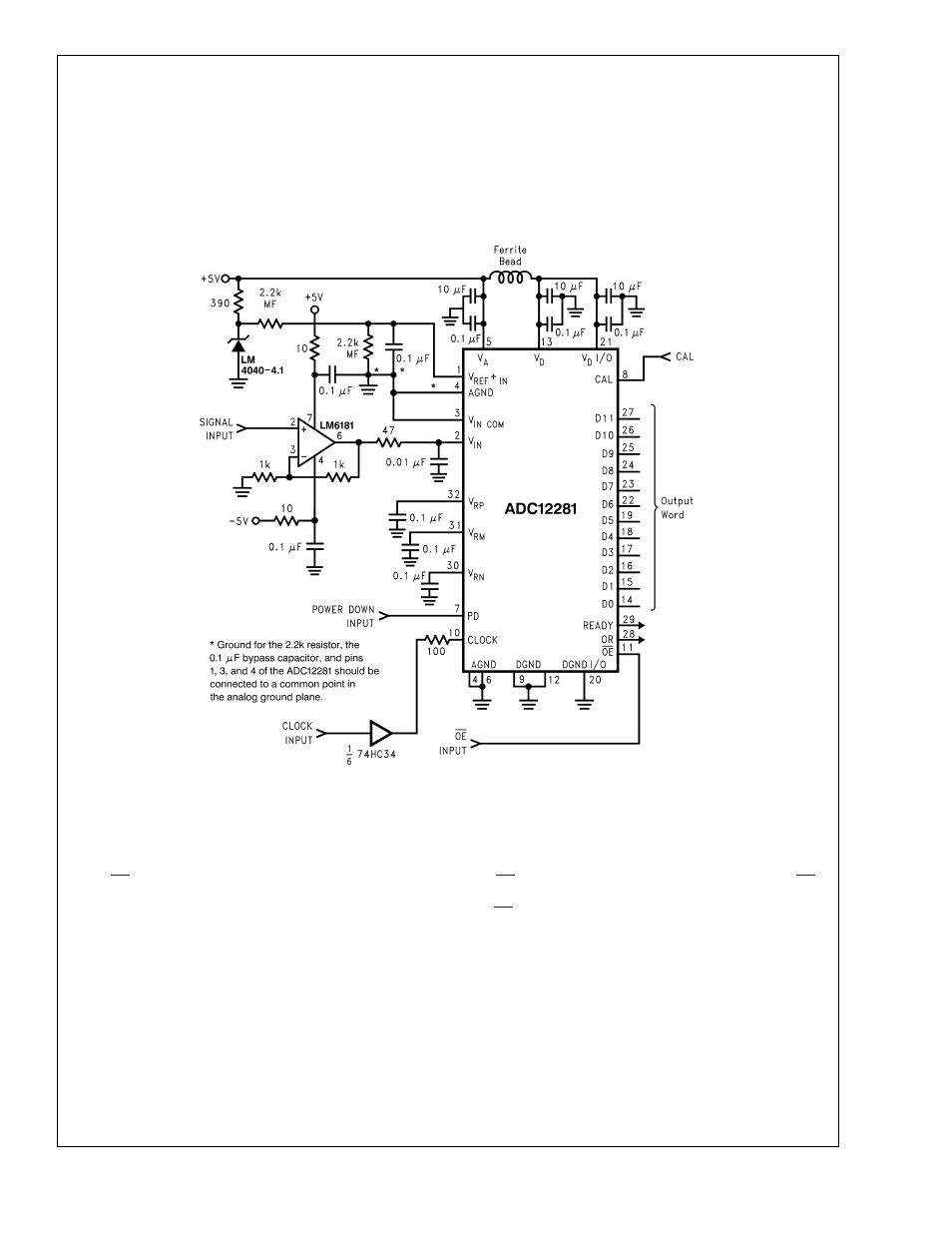
Applications Information
(Continued)
analog ground plane. The ground return for the reference
voltage should enter the ground plane at the same point as
does the V
IN COM
pin.
To simplify the interface, the ADC12281 has an internal
single-ended to differential buffer. This permits performance
you would expect to see with a differential input while driving
the input with a single-ended signal.
To achieve maximum performance, you should be careful to
maintain short input and ground runs in lines carrying signal
current. The signal ground line, V
IN COM
and the reference
ground should all enter the analog ground plane at the same
point, as indicated in Figure 5.
2.0 DIGITAL INPUTS
The ADC12281 has four digital inputs. They are CLOCK,
CAL, OE and PD.
The CLOCK input should be driven with a stable, low phase
jitter TTL level clock signal in the range of 0.5 MHz to 20
MHz. The clock high level should be limited to 3 V
P-P
for
maximum SNR performance and to meet data sheet perfor-
mance specifications. The trace carrying the clock signal
should be as short as possible. This trace should not cross
any other signal line, analog or digital, not even at 90˚.
The level sensitive CAL input must be pulsed high for at
least three clock cycles to begin ADC calibration. For best
performance, calibration should be performed about ten sec-
onds after power up, after resetting the ADC and whenever
the temperature has changed by more than 25˚C since the
last calibration cycle. Calibration should be performed at the
same clock frequency that will be used for conversions.
Calibration takes 4000 clock cycles to be performed. Irrel-
evant data may appear at the data outputs during CAL.
The OE pin is used to READ the conversion. When the OE
pin is low, the output buffers return to the active state. When
the OE input is high, the output buffers are in the high
impedance state.
The PD pin, when high, holds the ADC12281 in a
power-down mode where power consumption is typically
less than 15 mW to conserve power when the converter is
not being used. The ADC12281 will begin normal operation
with t
PD
after this pin is brought low, provided a valid CLOCK
input is present. The data in the pipeline is corrupted while in
the power-down mode. The ADC12281 does not have to be
re-calibrated after a power-down cycle unless the power
supply voltage or ambient temperature has changed.
10102728
FIGURE 5. Suggested Application Circuit
ADC12281
www.national.com
13