Absolute maximum ratings, Operating ratings (notes , ), Converter electrical characteristics – Rainbow Electronics ADC12281 User Manual
Page 5: Dc and logic electrical characteristics, Operating ratings
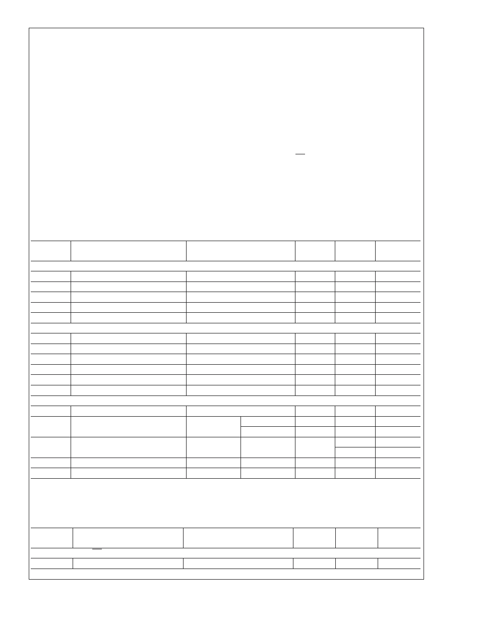
Absolute Maximum Ratings
(Notes 1,
If Military/Aerospace specified devices are required,
please contact the National Semiconductor Sales Office/
Distributors for availability and specifications.
Supply Voltages (V
A
, V
D
, V
D
I/O)
6.5V
|V
A
–V
D
|
≤100 mV
V
D
I/O–V
A
, V
D
I/O–V
D
≤300 mV
Voltage on Any Input or Output Pin
−0.3V to V
A
+0.3V
Input Current at Any Pin (Note 3)
±
25 mA
Package Input Current (Note 3)
±
50 mA
Power Dissipation at T
A
= 25˚C
See (Note 4)
ESD Susceptibility
Human Body Model (Note 5)
2500V
Machine Model (Note 5)
250V
Soldering Temperature, Infrared,
(10 sec.) (Note 6)
300˚C
Storage Temperature
−65˚C to +150˚C
Operating Ratings
(Notes 1, 2)
Operating Temperature Range
−40˚C
≤ T
A
≤
+85˚C
Supply Voltage (V
A
, V
D
)
+4.75V to +5.25V
Output Driver Supply Voltage (V
D
I/O)
+2.7V to V
D
V
REF
Input
1.8V to 2.2V
CLOCK, CAL, PD, OE
−0.05V to V
D
+0.05V
Ground Difference |AGND–DGND|
≤100 mV
Converter Electrical Characteristics
The following specifications apply for AGND = DGND = DGND I/O = 0V, V
A
= V
D
= V
D
I/O = +5V, PD = +5V, V
REF
= +2.0V,
f
CLK
= 20 MHz, 3 V
P-P
at 50% duty cycle, C
L
= 25 pF/pin. After Auto-Cal. Boldface limits apply for T
A
= T
J
= T
MIN
to T
MAX
;
all other limits T
A
= T
J
= 25˚C (Notes 7, 8, 9).
Symbol
Parameter
Conditions
Typical
Limits
Units
(Limits)
STATIC CONVERTER CHARACTERISTICS
Resolution with No Missing Codes
12
Bits (min)
INL
Integral Non-Linearity
±
1.0
±
2.5
LSB (max)
DNL
Differential Non-Linearity
±
0.35
±
0.9
LSB (max)
Full-Scale Error
+3
±
10
LSB (max)
Zero Error
+7
±
17
LSB (max)
DYNAMIC CONVERTER CHARACTERISTICS
BW
Full Power Bandwidth
100
MHz
SNR
Signal-to-Noise Ratio
f
IN
= 4.43 MHz, V
IN
= 2.0 V
P-P
65.5
62.5
dB (min)
SINAD
Signal-to-Noise and Distortion
f
IN
= 4.43 MHz, V
IN
= 2.0 V
P-P
65
62
dB (min)
ENOB
Effective Number of Bits
f
IN
= 4.43 MHz, V
IN
= 2.0 V
P-P
10.5
10
Bits (min)
THD
Total Harmonic Distortion
f
IN
= 4.43 MHz, V
IN
= 2.0 V
P-P
−76
dB
SFDR
Spurious Free Dynamic Range
f
IN
= 4.43 MHz, V
IN
= 2.0 V
P-P
75
dB
REFERENCE AND ANALOG INPUT CHARACTERISTICS
V
IN
Input Voltage Range
V
REF
V (max)
C
IN
V
IN
Input Capacitance
(CLK LOW)
10
pF
(CLK HIGH)
15
pF
V
REF
Reference Voltage (Note 14)
2.00
1.8
V (min)
2.2
V (max)
Reference Input Leakage Current
10
µA
Reference Input Resistance
1
M
Ω
DC and Logic Electrical Characteristics
The following specifications apply for AGND = DGND = DGND I/O = 0V, V
A
= V
D
= V
D
I/O = +5V, PD = +5V, V
REF
= +2.0V,
f
CLK
= 20 MHz, 3 V
P-P
at 50% duty cycle, C
L
= 25 pF/pin. After Auto-Cal. Boldface limits apply for T
A
= T
J
= T
MIN
to T
MAX
;
all other limits T
A
= T
J
= 25˚C (Notes 7, 8, 9).
Symbol
Parameter
Conditions
Typical
Limits
Units
(Limits)
CLOCK, CAL, PD, OE DIGITAL INPUT CHARACTERISTICS
V
IH
Logical “1” Input Voltage
V
D
= 5.25V
2.0
V (min)
ADC12281
www.national.com
5