Ac electrical characteristics, Note 3), Dc and logic electrical characteristics – Rainbow Electronics ADC12281 User Manual
Page 6
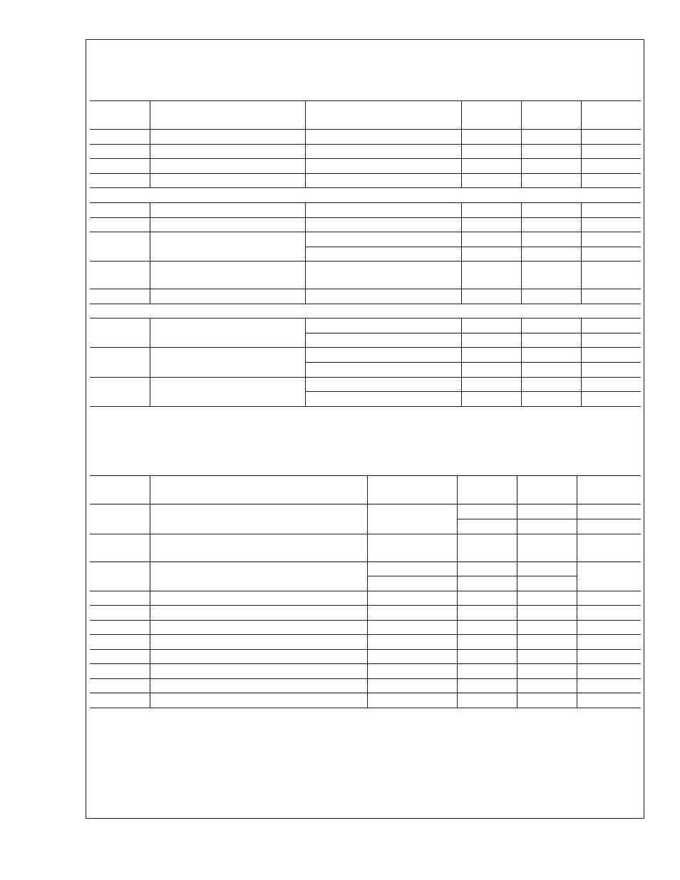
DC and Logic Electrical Characteristics
(Continued)
The following specifications apply for AGND = DGND = DGND I/O = 0V, V
A
= V
D
= V
D
I/O = +5V, PD = +5V, V
REF
= +2.0V,
f
CLK
= 20 MHz, 3 V
P-P
at 50% duty cycle, C
L
= 25 pF/pin. After Auto-Cal. Boldface limits apply for T
A
= T
J
= T
MIN
to T
MAX
;
all other limits T
A
= T
J
= 25˚C (Notes 7, 8, 9).
Symbol
Parameter
Conditions
Typical
Limits
Units
(Limits)
V
IL
Logical “0” Input Voltage
V
D
= 4.75V
0.8
V (max)
I
IH
Logical “1” Input Current
V
IN
= 5.0V
10
µA
I
IL
Logical “0” Input Current
V
IN
= 0V
−10
µA
C
IN
Logic Input Capacitance
8
pF
D0–D11 DIGITAL OUTPUT CHARACTERISTICS
V
OH
Logical “1” Output Voltage
I
OUT
= −1 mA
4
V (min)
V
OL
Logical “0” Output Voltage
I
OUT
= 1.6 mA
0.4
V (max)
I
OZ
TRI-STATE Output Current
V
OUT
= 3V or 5V
100
nA
V
OUT
= 0V
−100
nA
+I
SC
Output Short Circuit Source
Current
V
D
I/O = 3V, V
OUT
= 0V
−29
mA
−I
SC
Output Short Circuit Sink Current
V
D
I/O = 3V, V
OUT
= V
D
28
mA
POWER SUPPLY CHARACTERISTICS
I
A
Analog Supply Current
PD = DGND (active)
85
100
mA (max)
PD = V
D
I/O (power-down mode)
3.5
mA
I
D
Digital Supply Current
PD = DGND (active)
3.6
6
mA (max)
PD = V
D
I/O (power-down mode)
1
mA
Total Power Consumption
PD = DGND (active)
443
530
mW (max)
PD = V
D
I/O (power-down mode)
20
typ
AC Electrical Characteristics
The following specifications apply for AGND = DGND = DGND I/O = 0V, V
A
= V
D
= V
D
I/O = +5V, PD = +5V, V
REF
= +2.0V,
f
CLK
= 20 MHz, 3 V
P-P
at 50% duty cycle, C
L
= 25 pF/pin. After Auto-Cal. Boldface limits apply for T
A
= T
J
= T
MIN
to T
MAX
;
all other limits T
A
= T
J
= 25˚C (Notes 7, 8, 9).
Symbol
Parameter
Conditions
Typical
Limits
Units
(Limits)
f
CLK
Conversion Clock (CLOCK) Frequency
0.5
MHz (min)
20
MHz (max)
t
CONV
Conversion Latency
10
Clock
Cycles
t
OD
Data Output Delay after Rising CLK Edge
V
D
I/O = 3V
7
ns (max)
V
D
I/O = 5V
5
17
I
OZ
Data Outputs into TRI-STATE Mode
16
ns
t
OE
Data Outputs Active after TRI-STATE
10
ns
t
WCAL
Calibration Request Pulse Width
3
T
CLK
t
RDYC
Ready Low after CAL Request
3
T
CLK
t
CAL
Calibration Cycle
4000
T
CLK
t
WPD
Power-Down Pulse Width
3
T
CLK
t
RDYPD
Ready Low after PD Request
3
T
CLK
t
PD
Power-Down Mode Exit Cycle
4000
T
CLK
Note 1: “Absolute Maximum Ratings” indicate limits beyond which damage to the device may occur. Operating Ratings indicate conditions for which the device is
functional, but do not guarantee specific performance limits. For guaranteed specifications and test conditions, see the Electrical Characteristics. The guaranteed
specifications apply only for the test conditions listed. Some performance characteristics may degrade when the device is not operated under the listed test
conditions.
Note 2: All voltages are measured with respect to GND = AGND = DGND = DGND I/O = 0V, unless otherwise specified.
Note 3: When the input voltage at any pin exceeds the power supplies (that is, V
IN
<
AGND or V
IN
>
V
A
, V
D
or V
D
I/O), the current at that pin should be limited
to 25 mA. The 50 mA maximum package input current rating limits the number of pins that can safely exceed the power supplies with an input current of 25 mA to
two.
ADC12281
www.national.com
6