Typical performance characteristics, Note 9) – Rainbow Electronics ADC08351 User Manual
Page 6
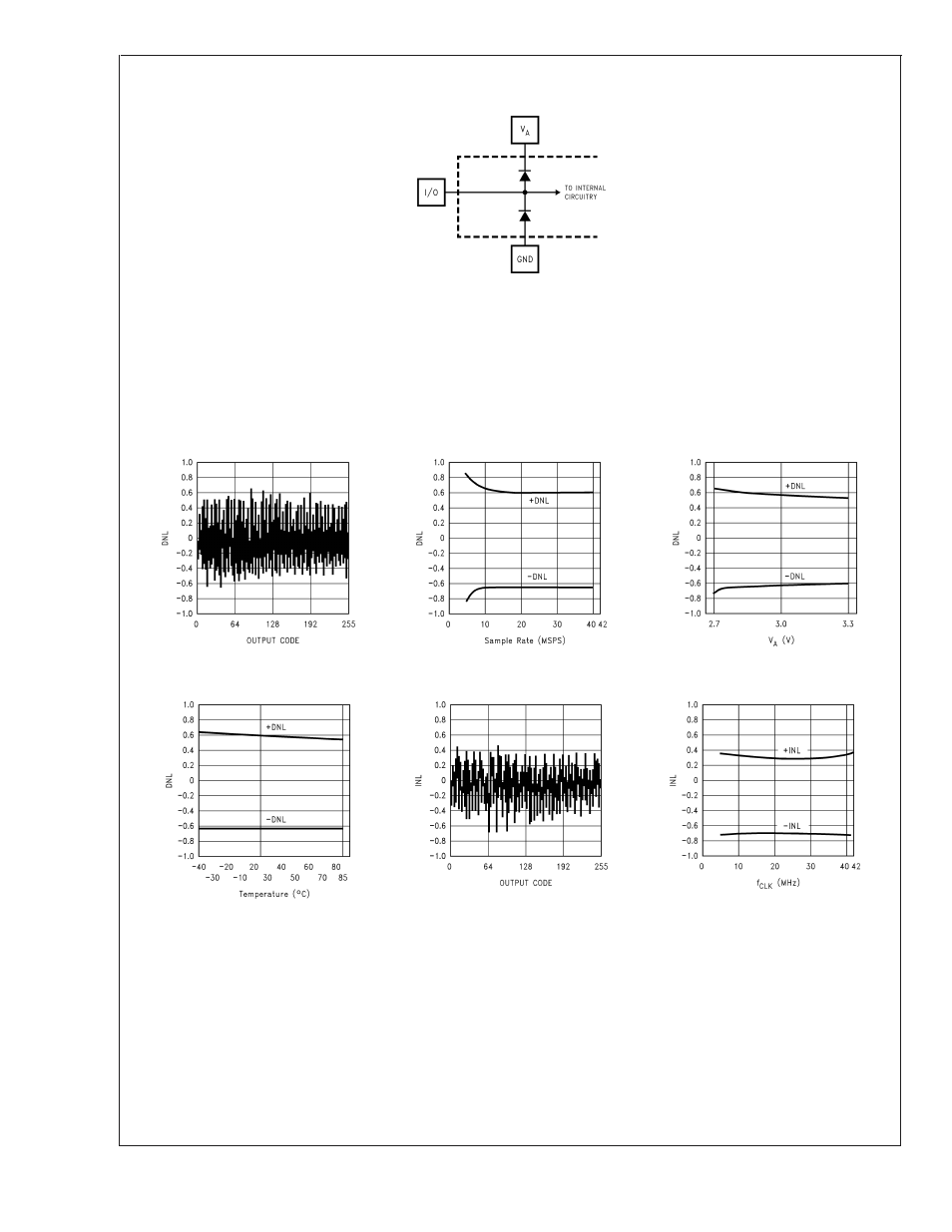
Note 7: All inputs are protected as shown below. Input voltage magnitudes up to 500 mV above the supply voltage or 500 mV below GND will not damage this
device. However, errors in the A/D conversion can occur if the input goes above V
A
or below AGND by more than 300 mV. As an example, if V
A
is 3.0 V
DC
, the
full-scale input voltage must be
≤3.3 V
DC
to ensure accurate conversions.
10089506
Note 8: To guarantee accuracy, it is required that V
A
and V
D
be well bypassed. Each V
A
and V
D
pin must be decoupled with separate bypass capacitors.
Note 9: Typical figures are at T
J
= 25˚C, and represent most likely parametric norms. Test limits are guaranteed to National’s AOQL (Average Outgoing Quality
Level).
Typical Performance Characteristics
V
A
= V
D
= V
D
I/O = 3V, f
CLK
= 42 MHz, unless otherwise
specified
DNL
@
42 MSPS
DNL vs Sample Rate
DNL vs V
A
10089507
10089508
10089509
DNL vs Temperature
INL
@
42 MSPS
INL vs Sample Rate
10089510
10089511
10089512
ADC08351
www.national.com
6