Ordering information, Adc08351 block diagram, Pin descriptions and equivalent circuits – Rainbow Electronics ADC08351 User Manual
Page 2
Ordering Information
ADC08351CIMTC
TSSOP
ADC08351CIMTCX
TSSOP (tape & reel)
ADC08351CILQ
LLP (tape & reel - 1, 000 units)
ADC08351CILQX
LLP (tape & reel - 4, 500 units)
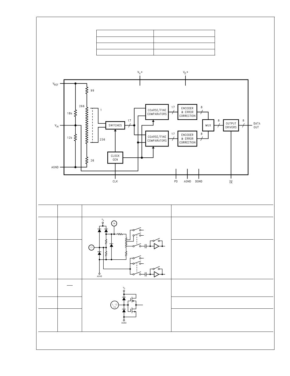
ADC08351 Block Diagram
10089502
Pin Descriptions and Equivalent Circuits
(LLP pins in parentheses)
Pin
No.
Symbol
Equivalent Circuit
Description
17
(17)
V
IN
Analog signal input. Conversion range is 0.5 V
P-P
to
0.68 V
A
.
14
(14)
V
REF
Positive reference voltage input. Operating range of
this voltage is 0.75V to V
A
. This pin should be
bypassed with a 10 µF tantalum or aluminum
electrolytic capacitor and a 0.1 µF ceramic chip
capacitor.
1
(22)
OE
CMOS/TTL compatible digital input that, when low,
enables the digital outputs of the ADC08351. When
high, the outputs are in a high impedance state.
12
(11)
CLK
CMOS/TTL compatible digital clock input. V
IN
is
sampled on the falling edge of CLK input.
15
(15)
PD
CMOS/TTL compatible digital input that, when high,
puts the ADC08351 into the power down mode,
where it consumes minimal power. When this pin is
low, the ADC08351 is in the normal operating mode.
ADC08351
www.national.com
2