Pin descriptions and equivalent circuits – Rainbow Electronics ADC08351 User Manual
Page 3
Pin Descriptions and Equivalent Circuits
(LLP pins in parentheses) (Continued)
Pin
No.
Symbol
Equivalent Circuit
Description
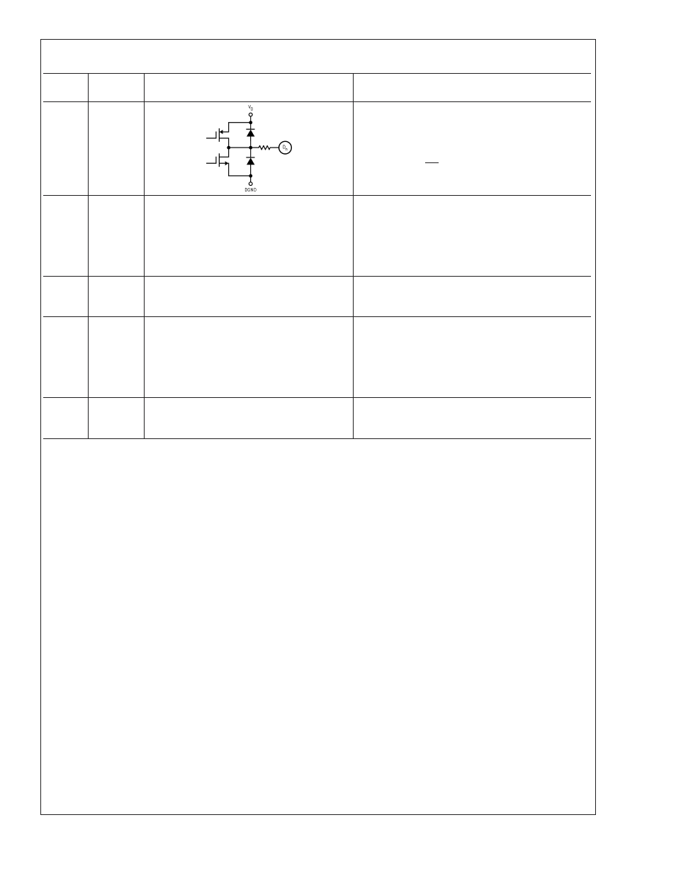
3 thru
10
(1 thru
8)
D0–D7
Conversion data digital output pins. D0 is the LSB,
D7 is the MSB. Valid data is output just after the
rising edge of the CLK input. These pins are enabled
by bringing the OE pin low.
11, 13
(10,
12)
V
D
Positive digital supply pin. Connect to a clean, quiet
voltage source of +3V. V
A
and V
D
should have a
common supply and be separately bypassed with a
10 µF tantalum or aluminum electrolytic capacitor and
a 0.1 µF ceramic chip capacitor. See Section 3.0 for
more information.
2, 20
(21,
23)
DGND
The ground return for the digital supply. AGND and
DGND should be connected together close to the
ADC08351.
16
(16)
V
A
Positive analog supply pin. Connected to a clean,
quiet voltage source of +3V. V
A
and V
D
should have
a common supply and be separately bypassed with a
10 µF tantalum or aluminum electrolytic capacitor and
a 0.1 µF ceramic chip capacitor. See Section 3.0 for
more information.
18, 19
(18,
19)
AGND
The ground return for the analog supply. AGND and
DGND should be connected together close to the
ADC08351 package.
ADC08351
www.national.com
3