0 power supply considerations, 0 layout and grounding, Applications information – Rainbow Electronics ADC08351 User Manual
Page 10
Applications Information
(All schematic
pin numbers refer to the TSSOP.) (Continued)
CLC440, LM6152, LM6154, LM6181 and LM6182 are good
devices for driving analog input of the ADC08351. Do not
drive the input beyond the supply rails.
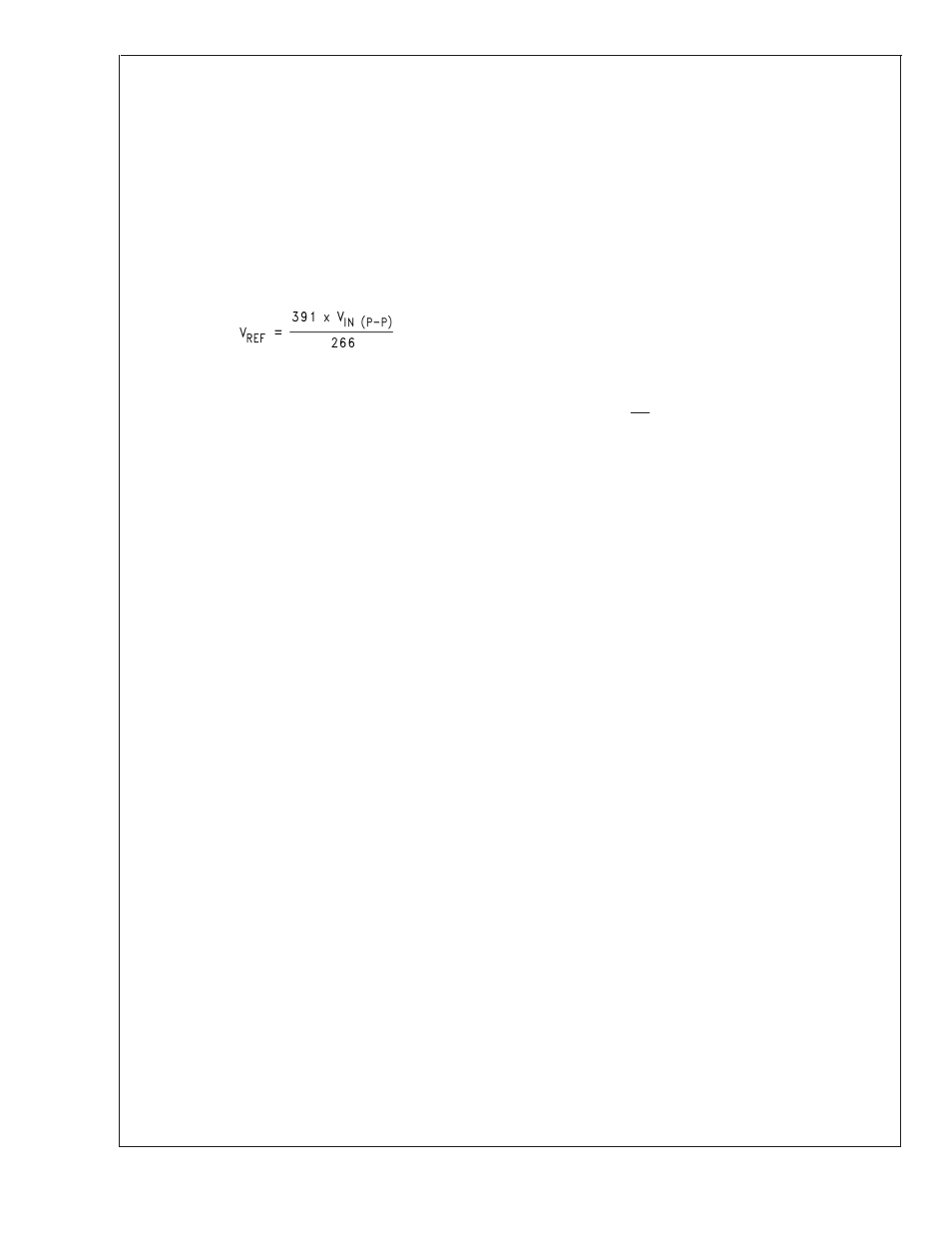
The maximum peak-to-peak input level without clipping of
the reconstructed output is determined by the values of the
resistor string between V
REF
and AGND. The bottom of the
reference ladder has a voltage of 0.0665 times V
REF
, while
the top of the reference ladder has a voltage of 0.7468 times
V
REF
. The maximum peak-to-peak input level works out to
be about 68% of the value of V
REF
. The relationship between
the input peak-to-peak voltage and V
REF
is
We do not recommend opertaing with input levels below
1 V
P-P
because the signal-to-noise ratio will degrade consid-
erably due to the quantization noise. However, the
ADC08351 will give adequate results in many applications
with signal levels down to about 0.5 V
P-P
(V
REF
= 0.735V).
Very good performance can be obtained with reference volt-
ages up to the supply voltage (V
A
= V
REF
= 3V, 2.04 V
P-P
).
As with all sampling ADCs, the opening and closing of the
switches associated with the sampling causes an output of
energy from the analog input, V
IN
. The reference ladder also
has switches associated with it, so the reference source
must be able to supply sufficient current to hold V
REF
steady.
The analog input of the ADC08351 is self-biased with an
18 k
Ω pull-up resistor to V
REF
and a 12 k
Ω pull-down resistor
to AGND. This allows for either a.c. or d.c. coupling of the
input signal. These two resistors provide a convenient way to
ensure a signal that is less than full scale will be centered
within the input common mode range of the converter. How-
ever, the high values of these resistors and the energy
coming from this input means that performance will be im-
proved with d.c. coupling.
The driving circuit at the signal input must be able to sink and
source sufficient current at the signal frequency to prevent
distortion from being introduced at the input.
2.0 POWER SUPPLY CONSIDERATIONS
A tantalum or aluminum electrolytic capacitor of 5 µF to
10 µF should be placed within a centimeter of each of the
A/D power pins, with a 0.1 µF ceramic chip capacitor placed
within
1
⁄
2
centimeter of each of the power pins. Leadless chip
capacitors are preferred because they provide lower lead
inductance than do their leaded counterparts.
While a single voltage source should be used for the analog
and digital supplies of the ADC08351, these supply pins
should be decoupled from each other to prevent any digital
noise from being coupled to the analog power pins. A ferrite
bead between the analog and digital supply pins would help
to isolate the two supplies.
The converter digital supply should not be the supply that is
used for other digital circuitry on the board. It should be the
same supply used for the A/D analog supply, decoupled from
the A/D analog supply pin, as described above. A common
analog supply should be used for both V
A
and V
D
, and each
of these pins should be separately bypassed with a 0.1 µF
ceramic capacitor and with low ESR a 10 µF capacitor.
As is the case with all high speed converters, the ADC08351
is sensitive to power supply noise. Accordingly, the noise on
the analog supply pin should be minimized, keeping it below
200 mV
P-P
at 100 kHz. Of course, higher frequency noise on
the power supply should be even more severely limited.
No pin should ever have a voltage on it that is in excess of
the supply voltages. This can be a problem upon application
of power to a circuit. Be sure that the supplies to circuits
driving the CLK, OE, analog input and reference pins do not
come up any faster than does the voltage at the ADC08351
power pins.
3.0 LAYOUT AND GROUNDING
Proper grounding and proper routing of all signals is essen-
tial to ensure accurate conversion. Separate analog and
digital ground planes that are connected beneath the
ADC08351 are required to meet data sheet limits. The ana-
log and digital grounds may be in the same layer, but should
be separated from each other and should never overlap
each other.
Capacitive coupling between the typically noisy digital
ground plane and the sensitive analog circuitry can lead to
poor performance that may seem impossible to isolate and
remedy. The solution is to keep the analog circuitry well
separated from the digital circuitry and from the digital
ground plane.
The back of the LLP package has a large metal area inside
the area bounded by the pins. This metal area is connected
to the die substrate (ground). This pad may be left floating if
desired. If it is connected to anything, it should be to ground
near the connection between analog and digital ground
planes. Soldering this metal pad to ground will help keep the
die cooler and could yield improved performance because of
the lower impedance between die and board grounds. How-
ever, a poor layout could compromise performance.
ADC08351
www.national.com
10