Absolute maximum ratings, Recommended operating conditions, Electrical characteristics – Rainbow Electronics DS90CP22 User Manual
Page 2: Ds90cp22
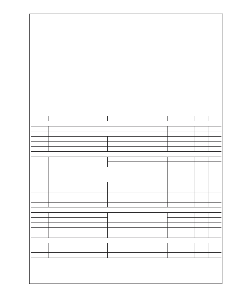
Absolute Maximum Ratings
If Military/Aerospace specified devices are required,
please contact the National Semiconductor Sales Office/
Distributors for availability and specifications.
Supply Voltage (V
CC
)
−0.3V to +4V
CMOS/TTL Input Voltage (EN0,
EN1, SEL0, SEL1)
−0.3V to (V
CC
+ 0.3V)
LVDS Receiver Input Voltage
(IN+, IN−)
−0.3V to +4V
LVDS Driver Output Voltage
(OUT+, OUT−)
−0.3V to +4V
LVDS Output Short Circuit
Current
Continuous
Junction Temperature
+150˚C
Storage Temperature Range
−65˚C to +150˚C
Lead Temperature
(Soldering, 4 sec.)
+260˚C
Maximum Package Power Dissipation at 25˚C
16L SOIC
1.435 W
16L SOIC Package Derating
11.48 mW/˚C above +25˚C
16L TSSOP
0.866 W
16L TSSOP Package Derating
9.6 mW/˚C above +25˚C
ESD Rating:
(HBM, 1.5k
Ω, 100pF)
>
5 kV
(EIAJ, 0
Ω, 200pF)
>
250 V
Recommended Operating
Conditions
Min Typ Max Units
Supply Voltage (V
CC
)
3.0
3.3
3.6
V
Receiver Input Voltage
0
V
CC
V
Operating Free Air Temperature
-40
+25 +85
˚C
Electrical Characteristics
Over recommended operating supply and temperature ranges unless otherwise specified
Symbol
Parameter
Conditions
Min
Typ
Max
Units
CMOS/TTL DC SPECIFICATIONS (EN0,EN1,SEL0,SEL1)
V
IH
High Level Input Voltage
2.0
V
CC
V
V
IL
Low Level Input Voltage
GND
0.8
V
I
IH
High Level Input Current
V
IN
= 3.6V or 2.0V; V
CC
= 3.6V
+7
+20
µA
I
IL
Low Level Input Current
V
IN
= 0V or 0.8V; V
CC
= 3.6V
±
1
±
10
µA
V
CL
Input Clamp Voltage
I
CL
= −18 mA
−0.8
−1.5
V
LVDS OUTPUT DC SPECIFICATIONS (OUT0,OUT1)
V
OD
Differential Output Voltage
R
L
= 75
Ω
270
365
475
mV
R
L
= 75
Ω, V
CC
= 3.3V, T
A
= 25˚C
285
365
440
mV
∆V
OD
Change in V
OD
between Complimentary Output States
35
mV
V
OS
Offset Voltage (Note 3)
1.0
1.2
1.45
V
∆V
OS
Change in V
OS
between Complimentary Output States
35
mV
I
OZ
Output TRI-STATE
®
Current
TRI-STATE Output,
±
1
±
10
µA
V
OUT
= V
CC
or GND
I
OFF
Power-Off Leakage Current
V
CC
= 0V; V
OUT
= 3.6V or GND
±
1
±
10
µA
I
OS
Output Short Circuit Current
V
OUT+
OR V
OUT−
= 0V
−15
−25
mA
I
OSB
Both Outputs Short Circuit Current
V
OUT+
AND V
OUT−
= 0V
−30
−50
mA
LVDS RECEIVER DC SPECIFICATIONS (IN0,IN1)
V
TH
Differential Input High Threshold
V
CM
= +0.05V or +1.2V or +3.25V,
0
+100
mV
V
TL
Differential Input Low Threshold
Vcc = 3.3V
−100
0
mV
V
CMR
Common Mode Voltage Range
V
ID
= 100mV, Vcc = 3.3V
0.05
3.25
V
I
IN
Input Current
V
IN
= +3.0V, V
CC
= 3.6V or 0V
±
1
±
10
µA
V
IN
= 0V, V
CC
= 3.6V or 0V
±
1
±
10
µA
SUPPLY CURRENT
I
CCD
Total Supply Current
R
L
= 75
Ω, C
L
= 5 pF,
EN0 = EN1 = High
98
125
mA
I
CCZ
TRI-STATE Supply Current
EN0 = EN1 = Low
43
55
mA
Note 1: “Absolute Maximum Ratings” are these beyond which the safety of the device cannot be guaranteed. They are not meant to imply that the device should
be operated at these limits. The table of “Electrical Characteristics” provides conditions for actual device operation.
Note 2: All typical are given for V
CC
= +3.3V and T
A
= +25˚C, unless otherwise stated.
Note 3: V
OS
is defined and measured on the ATE as (V
OH
+ V
OL
) / 2.
DS90CP22
www.national.com
2