Clock and calendar, Table 1. timekeeping registers and sram – Rainbow Electronics DS1375 User Manual
Page 6
to location 00h, the current time is transferred to a sec-
ond set of registers. The time information is read from
these secondary registers, while the clock may contin-
ue to run. This eliminates the need to reread the regis-
ters in case the main registers update during a read.
Note: Unless otherwise specified, the state of the regis-
ters is not defined when power is first applied.
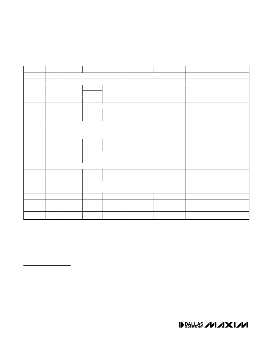
Clock and Calendar
The time and calendar information is obtained by read-
ing the appropriate register bytes.
Table
1 shows the
RTC registers. The time and calendar data are set or
initialized by writing the appropriate register bytes. The
contents of the time and calendar registers are in the
binary-coded decimal (BCD) format. The DS1375 can
be run in either 12-hour or 24-hour mode. Bit 6 of the
hours register is defined as the 12- or 24-hour mode
select bit. When high, the 12-hour mode is selected. In
the 12-hour mode, bit 5 is the AM/PM bit with logic high
being PM. In the 24-hour mode, bit 5 is the second 10-
hour bit (20–23 hours). The century bit (bit 7 of the
month register) is toggled when the years register over-
flows from 99 to 00.
The day-of-week register increments at midnight.
Values that correspond to the day of week are user-
defined but must be sequential (i.e., if 1 equals
Sunday, then 2 equals Monday, and so on). Illogical
time and date entries result in undefined operation.
When reading or writing the time and date registers,
secondary (user) buffers are used to prevent errors
when the internal registers update. When reading the
time and date registers, the user buffers are synchro-
nized to the internal registers on any START or STOP
and when the register pointer rolls over to zero. The
time information is read from these secondary registers,
while the clock continues to run. This eliminates the
need to reread the registers in case the main registers
update during a read.
DS1375
2-Wire Digital Input RTC with Alarm
6
_____________________________________________________________________
Table
1. Timekeeping Registers and SRAM
ADDRESS
BIT 7
BIT 6
BIT 5
BIT 4
BIT 3
BIT 2
BIT 1
BIT 0
FUNCTION
RANGE
00h
0
10 Seconds
Seconds
Seconds
00–59
01h
0
10 Minutes
Minutes
Minutes
00–59
AM/PM
02h
0
12/24
10 Hours
10 Hours
Hours
Hours
1–12 + AM/PM
00–23
03h
0
0
0
0
0
Day
Day
1–7
04h
0
0
10 Date
Date
Date
00–31
05h
Century
0
0
10
Month
Months
Month/
Century
01–12 +
Century
06h
10 Year
Year
Year
00–99
07h
A1M1
10 Seconds
Seconds
Alarm 1 Seconds
00–59
08h
A1M2
10 Minutes
Minutes
Alarm 1 Minutes
00–59
AM/PM
09h
A1M3
12/24
10 Hours
10 Hours
Hours
Alarm 1 Hours
1–12 + AM/PM
00–23
Day
Alarm 1 Day
1–7
0Ah
A1M4
DY/DT
10 Date
Date
Alarm 1 Date
1–31
0Bh
A2M2
10 Minutes
Minutes
Alarm 2 Minutes
00–59
AM/PM
0Ch
A2M3
12/24
10 Hours
10 Hours
Hours
Alarm 2 Hours
1–12 + AM/PM
00–23
—
Day
Alarm 2 Day
1–7
0Dh
A2M4
DY/DT
10 Date
Date
Alarm 2 Date
1–31
0Eh
ECLK
CLKSEL1
CLKSEL0
RS2
RS1
INTCN
A2IE
A1IE
Control
—
0Fh
0
0
0
0
0
0
A2F
A1F
Control/
Status
—
10h–1Fh
B7
B6
B5
B4
B3
B2
B1
B0
SRAM
00–FFH