Rainbow Electronics DS1375 User Manual
Page 2
DS1375
2-Wire Digital Input RTC with Alarm
2
_____________________________________________________________________
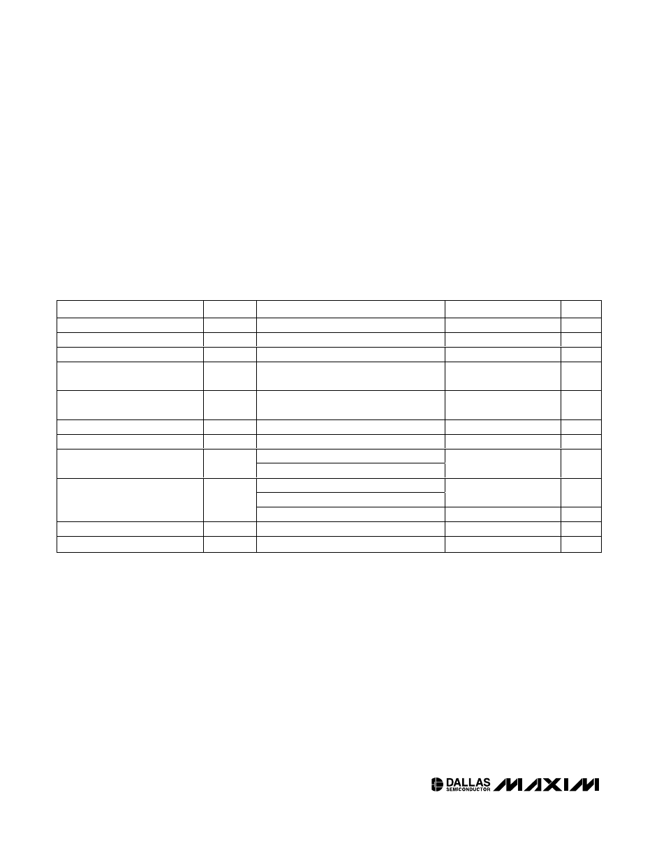
ABSOLUTE MAXIMUM RATINGS
RECOMMENDED DC OPERATING CONDITIONS
(V
CC
= +1.7V to +5.5V, T
A
= -40°C to +85°C, unless otherwise noted. Typical values are at V
CC
= 3.3V, T
A
= +25°C, unless other-
wise noted.) (Note 1)
Stresses beyond those listed under “Absolute Maximum Ratings” may cause permanent damage to the device. These are stress ratings only, and functional
operation of the device at these or any other conditions beyond those indicated in the operational sections of the specifications is not implied. Exposure to
absolute maximum rating conditions for extended periods may affect device reliability.
Note 1:
Limits at -40°C are guaranteed by design and not production tested.
Note 2:
All voltages are referenced to ground.
Note 3:
For the CLK pin, input voltages above V
CC
+ 0.3V cause current to flow into the device. The input current must not
exceed the current drawn by the circuit that is connected to V
CC
. Otherwise, current flows out of the DS1375, raising the
voltage level on the V
CC
bus.
Note 4:
V
IL MIN
on the CLK pin can exceed -0.3V as long as the current is limited to less than 1mA.
Note 5:
I
CCA
—SCL clocking at max frequency = 400kHz.
Note 6:
CLK pin running at 32,768Hz, rise and fall times at 10ns or less.
Note 7:
Specified with 2-wire bus inactive.
Voltage Range on V
CC
Pin
Relative to Ground.............................................-0.3V to +6.0V
Voltage Range on SDA, SCL, and WDS
Relative to Ground ....................................-0.3V to V
CC
+ 0.3V
Operating Temperature Range ...........................-40°C to +85°C
Storage Temperature Range .............................-55°C to +125°C
Soldering Temperature .......................................See IPC/JEDEC
J-STD-020A Specification
PARAMETER
SYMBOL
CONDITIONS
MIN
TYP
MAX
UNITS
Supply Voltage
V
CC
(Note 2)
1.7
3.3
5.5
V
Timekeeping Voltage
V
TK
(Note 2)
1.3
5.5
V
Input Logic 1 (SDA, SCL)
V
IH
(Note 2)
0.7 x V
CC
V
CC
+ 0.3
V
Supply Voltage, Pullup
(SQW/INT, CLK)
V
PULLUP
(Notes 2, 3)
5.5
V
Input Logic 0
V
IL
(Notes 2, 4)
-0.3
+0.3
V
CC
V
Input Leakage (SCL, CLK)
I
LI
-1
+1
µA
I/O Leakage (SDA, SQW/INT)
I
LO
-1
+1
µA
V
CC
> 2V; V
OL
= 0.4V
SDA Logic 0 Output
I
OLSDA
V
CC
< 2V; V
OL
= 0.2 x V
CC
3.0
mA
V
CC
> 2V; V
OL
= 0.4V
1.7V < V
CC
< 2V; V
OL
= 0.2 x V
CC
3.0
mA
SQW/INT Logic 0 Output
I
OLSQW
1.3V < V
CC
< 1.7V; V
OL
= 0.2 x V
CC
250
µA
Active Supply Current
I
CCA
(Notes 5, 6)
33
150
µA
Standby Current
I
CCS
(Notes 6, 7)
150
500
nA