Ac electrical characteristics – Rainbow Electronics DS1371 User Manual
Page 3
DS1371
3 of 14
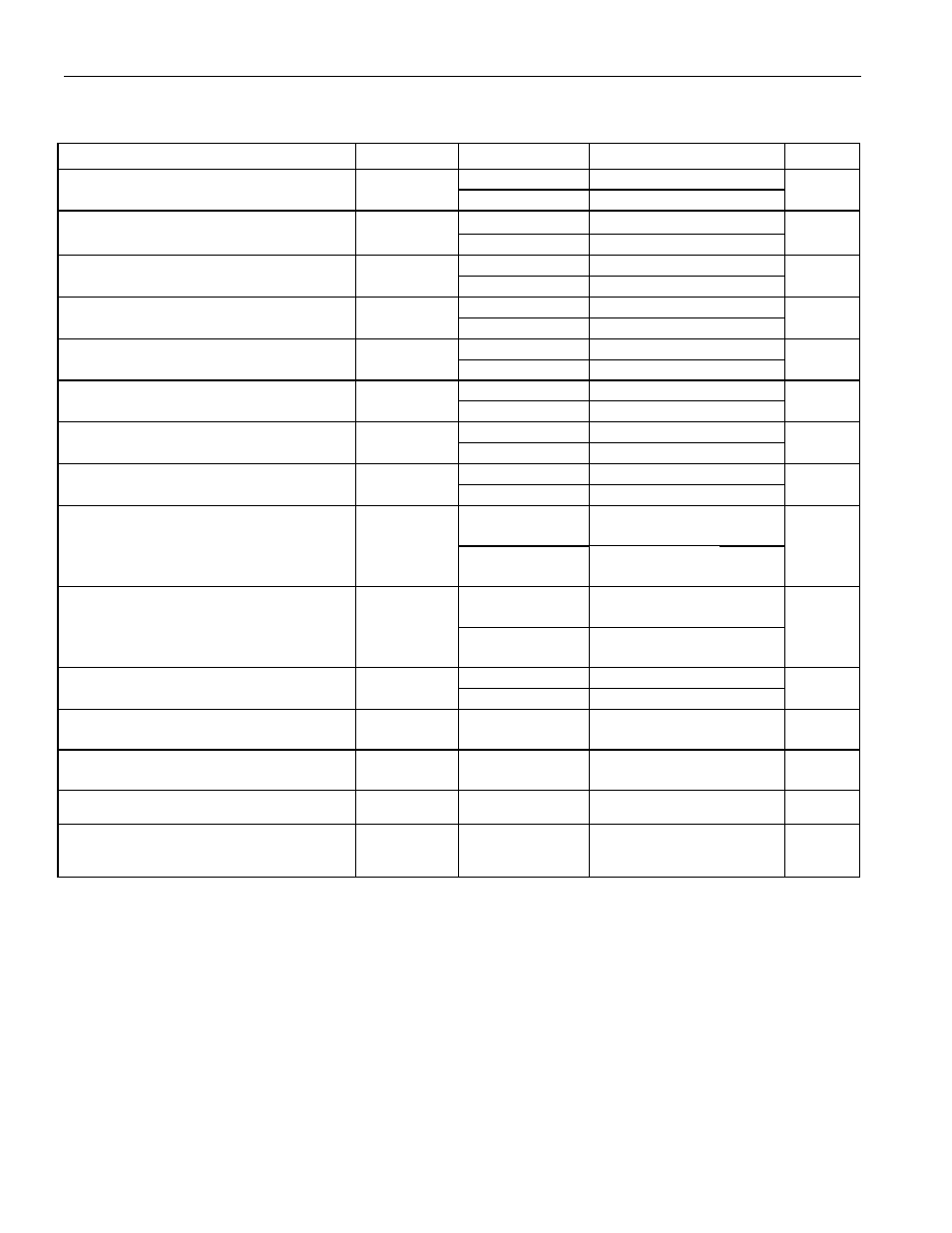
AC ELECTRICAL CHARACTERISTICS
(V
CC
= 1.7V to 5.5V, T
A
= -40°C to +85°C, unless otherwise noted.) (Note 8)
PARAMETER SYMBOL
CONDITIONS
MIN
TYP
MAX
UNITS
Fast mode
100
400
SCL Clock Frequency (Note 9)
f
SCL
Standard mode
0
100
kHz
Fast mode
1.3
Bus Free Time Between STOP and
START Conditions
t
BUF
Standard mode
4.7
ms
Fast mode
0.6
Hold Time (repeated) START Condition
(Note 10)
t
HD:STA
Standard mode
4.0
ms
Fast mode
1.3
Low Period of SCL Clock
t
LOW
Standard mode
4.7
ms
Fast mode
0.6
High Period of SCL Clock
t
HIGH
Standard mode
4.0
ms
Fast mode
0
0.9
Data Hold Time (Notes 11, 12)
t
HD:DAT
Standard mode
0
0.9
ms
Fast mode
100
Data Setup Time (Note 13)
t
SU:DAT
Standard mode
250
ns
Fast mode
0.6
Start Setup Time
t
SU:STA
Standard mode
4.7
ms
Fast mode
20 +
0.1C
B
300
Rise Time of Both SDA and SCL
Signals (Note 9)
t
R
Standard mode
20 +
0.1C
B
1000
ns
Fast mode
20 +
0.1C
B
300
Fall Time of Both SDA and SCL Signals
(Note 9)
t
F
Standard mode
20 +
0.1C
B
300
ns
Fast mode
0.6
Setup Time for STOP Condition
t
SU:STO
Standard mode
4.7
ms
Capacitive Load for Each Bus Line
(Note 7)
C
B
400 pF
Pulse Width of Spikes that Must be
Suppressed by the Input Filter (Note 14)
T
SP
Fast
mode
30 ns
Watchdog Strobe (WDS) Pulse Width
t
WDS
100 ns
Oscillator Stop Flag (OSF) Delay
(Note 8)
t
OSF
100 ms
Note 1: All voltages are referenced to ground.
Note 2: SCL and WDS only.
Note 3: SDA and SQW/
INT.
Note 4: Limits at -40
°C are guaranteed by design and not production tested.
Note 5: I
CCA
—SCL clocking at max frequency = 400kHz. WDS inactive.
Note 6: Specified with WDS input and 2-wire bus inactive, SCL = SDA = V
CC
.
Note 7: Measured with a 32.768kHz crystal attached to the X1 and X2 pins.
Note 8: The parameter t
OSF
is the period of time the oscillator must be stopped in order for the OSF flag to be set over the voltage range of 1.3V
≤ V
CC
≤ V
CCMAX
.
Note 9: A fast mode device can be used in a standard mode system, but the requirement t
SU:DAT
≥ to 250ns must then be met. This is
automatically the case if the device does not stretch the LOW period of the SCL signal. If such a device does stretch the LOW period of
the SCL signal, it must output the next data bit to the SDA line t
R MAX
+
t
SU:DAT
= 1000 + 250 = 1250ns before the SCL line is released.
Note 10: After this period, the first clock pulse is generated.
Note 11: A device must internally provide a hold time of at least 300ns for the SDA signal (referred to the V
IHMIN
of the SCL signal) in order to
bridge the undefined region of the falling edge of SCL.
Note 12: The maximum t
HD:DAT
has only to be met if the device does not stretch the LOW period (t
LOW
) of the SCL signal.
Note 13: C
B
—total capacitance of one bus line in pF.
Note 14: This parameter is not production tested.