At89ls53, Programmable watchdog timer – Rainbow Electronics AT89LS53 User Manual
Page 9
AT89LS53
4-257
Data Memory - RAM
The AT89LS53 implements 256 bytes of RAM. The upper
128 bytes of RAM occupy a parallel space to the Special
Function Registers. That means the upper 128 bytes have
the same addresses as the SFR space but are physically
separate from SFR space.
When an instruction accesses an internal location above
address 7FH, the address mode used in the instruction
specifies whether the CPU accesses the upper 128 bytes
of RAM or the SFR space. Instructions that use direct
addressing access SFR space.
For example, the following direct addressing instruction
accesses the SFR at location 0A0H (which is P2).
MOV 0A0H, #data
Instructions that use indirect addressing access the upper
128 bytes of RAM. For example, the following indirect
addressing instruction, where R0 contains 0A0H, accesses
the data byte at address 0A0H, rather than P2 (whose
address is 0A0H).
MOV @R0, #data
Note that stack operations are examples of indirect
addressing, so the upper 128 bytes of data RAM are avail-
able as stack space.
Programmable Watchdog Timer
The programmable Watchdog Timer (WDT) operates from
an independent oscillator. The prescaler bits, PS0, PS1
and PS2 in SFR WCON are used to set the period of the
Watchdog Timer from 16 ms to 2048 ms. The available
timer periods are shown in the following table and the
actual timer periods (at V
CC
= 5V) are within
±
30% of the
nominal.
The WDT is disabled by Power-on Reset and during Power
Down. It is enabled by setting the WDTEN bit in SFR
WCON (address = 96H). The WDT is reset by setting the
WDTRST bit in WCON. When the WDT times out without
being reset or disabled, an internal RST pulse is generated
to reset the CPU.
Table 7. Watchdog Timer Period Selection
WDT Prescaler Bits
Period (nominal)
PS2
PS1
PS0
0
0
0
16 ms
0
0
1
32 ms
0
1
0
64 ms
0
1
1
128 ms
1
0
0
256 ms
1
0
1
512 ms
1
1
0
1024 ms
1
1
1
2048 ms
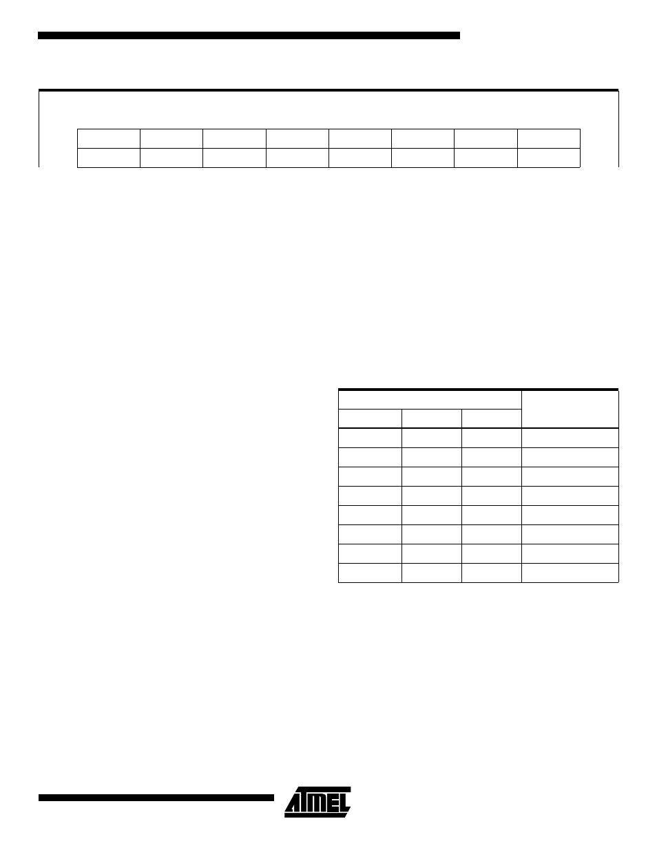
Table 6. SPDR—SPI Data Register
SPDR Address = 86H
Reset Value = unchanged
SPD7
SPD6
SPD5
SPD4
SPD3
SPD2
SPD1
SPD0
Bit
7
6
5
4
3
2
1
0