At89ls53 – Rainbow Electronics AT89LS53 User Manual
Page 15
AT89LS53
4-263
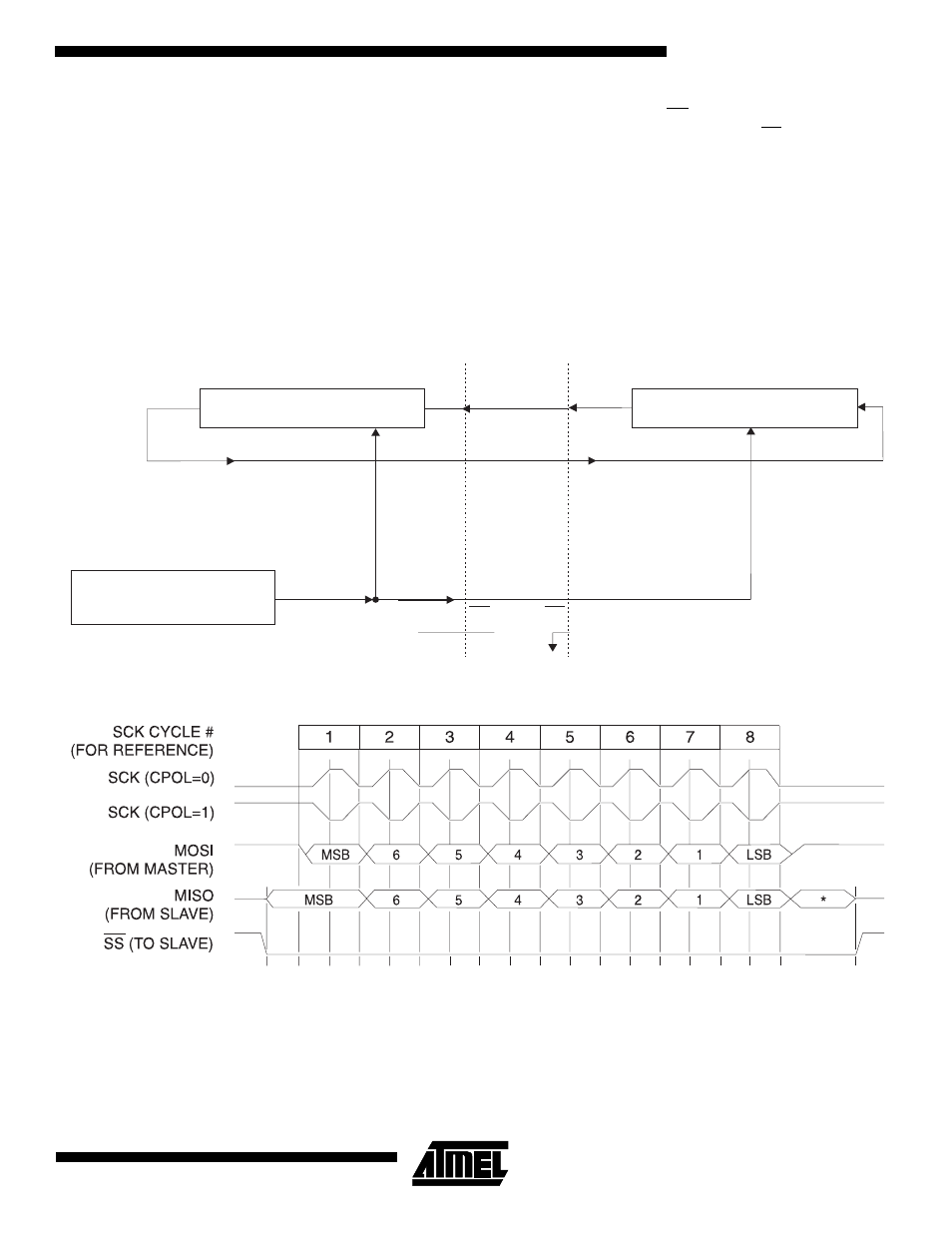
The interconnection between master and slave CPUs with
SPI is shown in the following figure. The SCK pin is the
clock output in the master mode but is the clock input in the
slave mode. Writing to the SPI data register of the master
CPU starts the SPI clock generator, and the data written
shifts out of the MOSI pin and into the MOSI pin of the
slave CPU. After shifting one byte, the SPI clock generator
stops, setting the end of transmission flag (SPIF). If both
the SPI interrupt enable bit (SPIE) and the serial port inter-
rupt enable bit (ES) are set, an interrupt is requested.
The Slave Select input, SS/P1.4, is set low to select an
individual SPI device as a slave. When SS/P1.4 is set high,
the SPI port is deactivated and the MOSI/P1.5 pin can be
used as an input.
There are four combinations of SCK phase and polarity
with respect to serial data, which are determined by control
bits CPHA and CPOL. The SPI data transfer formats are
shown in Figures 8 and 9.
Figure 7. SPI Master-Slave Interconnection
8-BIT SHIFT REGISTER
MASTER
MISO
CLOCK GENERATOR
SPI
8-BIT SHIFT REGISTER
SLAVE
MISO
MOSI MOSI
SCK
SCK
SS
SS
V
CC
MSB
LSB
MSB
LSB
Figure 8. SPI transfer Format with CPHA = 0
*Not defined but normally MSB of character just received