At89ls53, Uart, Serial peripheral interface – Rainbow Electronics AT89LS53 User Manual
Page 14: Programmable clock out
AT89LS53
4-262
Programmable Clock Out
A 50% duty cycle clock can be programmed to come out on
P1.0, as shown in Figure 5. This pin, besides being a regu-
lar I/0 pin, has two alternate functions. It can be pro-
grammed to input the external clock for Timer/Counter 2 or
to output a 50% duty cycle clock ranging from 61 Hz to 3
MHz at a 12
MHz operating frequency.
To configure the Timer/Counter 2 as a clock generator, bit
C/T2 (T2CON.1) must be cleared and bit T2OE (T2MOD.1)
must be set. Bit TR2 (T2CON.2) starts and stops the timer.
The clock-out frequency depends on the oscillator fre-
quency and the reload value of Timer 2 capture registers
(RCAP2H, RCAP2L), as shown in the following equation.
In the clock-out mode, Timer 2 rollovers will not generate
an interrupt. This behavior is similar to when Timer 2 is
used as a baud-rate generator. It is possible to use Timer 2
as a baud-rate generator and a clock generator simulta-
neously. Note, however, that the baud-rate and clock-out
frequencies cannot be determined independently from one
another since they both use RCAP2H and RCAP2L.
UART
The UART in the AT89LS53 operates the same way as the
UART in the AT89C51, AT89C52 and AT89C55. For fur-
ther information, see the October 1995 Atmel Microcontrol-
ler Data Book, page 2-49, section titled, “Serial Interface.”
Serial Peripheral Interface
The serial peripheral interface (SPI) allows high-speed syn-
chronous data transfer between the AT89LS53 and periph-
eral devices or between several AT89LS53 devices. The
AT89LS53 SPI features include the following:
• Full-Duplex, 3-Wire Synchronous Data Transfer
• Master or Slave Operation
• 1.5-MHz Bit Frequency (max.)
• LSB First or MSB First Data Transfer
• Four Programmable Bit Rates
• End of Transmission Interrupt Flag
• Write Collision Flag Protection
• Wakeup from Idle Mode (Slave Mode Only)
Clock-Out Frequency
Oscillator Frequency
4
65536
RCAP2H,RCAP2L
(
)
–
[
]
×
-------------------------------------------------------------------------------------------
=
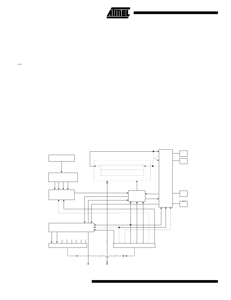
Figure 6. SPI Block Diagram
OSCILLATOR
8/16-BIT SHIFT REGISTER
READ DATA BUFFER
PIN CONTR
OL LOGIC
SPI CONTROL
SPI STATUS REGISTER
SPI INTERRUPT
REQUEST
INTERNAL
DATA BUS
SELECT
SPI CLOCK (MASTER)
DIVIDER
ч4ч16ч64ч128
SPI CONTROL REGISTER
8
8
8
SPIF
WCOL
SPR1
MSTR
SPIE
CLOCK
LOGIC
CLOCK
MSB
S
M
SPE
DORD
MSTR
CPOL
CPHA
SPR1
SPR0
MSTR
SPE
DORD
LSB
S
M
M
S
MISO
P1.6
MOSI
P1.5
SCK
1.7
SS
P1.4
SPR0
SPE