Rainbow Electronics DS1667 User Manual
Page 5
DS1667
021492 5/11
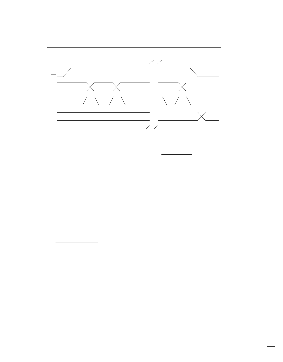
READING DATA Figure 4
RST
CLK
CONTROL
REGISTERS
CURRENT SETTINGS
NO
BIT 16
C
OUT
BIT 15
BIT 14
BIT 0
BIT 16
CHANGES
DS1667 LINEARITY MEASUREMENTS
An important specification for the DS1667 is linearity,
that is, for a given digital input, how close the analog out-
put is to that which is expected.
The test circuit used to measure the linearity of the
DS1667 is shown in Figure 5. Note that to get an accu-
rate output voltage it is necessary to assure that the out-
put current is 0, in order to negate the effects of wiper
impedance RW which is typically 400 ohms. For any
given setting N for the pot, the expected voltage output
at SOUT is:
VO = -5 + [10 X (N/256)] (in volts)
Absolute linearity is a comparison of the actual mea-
sured output voltage versus the expected value given
by the equation above, and is given in terms of an LSB,
which is the change in expected output when the digital
input is incremented by 1. In this case the LSB is 10/256
or 0.03906 volts. The equation for the absolute linearity
of the DS1667 is:
V
O
(actual)
*
V
O
(expected)
LSB
+
AL (in LSBs)
The specification for absolute linearity of the DS1667 is
+ 1 LSB typical.
Relative linearity is a comparison of the difference of ac-
tual output voltages of two successive taps and the dif-
ference of the expected output voltages of two succes-
sive taps. The expected difference of output voltages is
1 LSB or 0.03906V for the measurement system of Fig-
ure 5. Relative linearity is expressed in terms of an LSB
and is given by the equation:
D
V
O
(actual)
*
LSB
LSB
+
RL
The specification for relative linerity of the DS1667 is
+ 0.5 LSB typical.
Figure 6 is a plot of absolute linearity (AL) and relative
linearity (RL) versus wiper setting for a typical DS1667
at 25
°
C.
DESCRIPTION AND OPERATION - OP AMP
SECTION
The DS1667 contains two operational amplifiers which
are ideal for operation from a single 5V supply and
ground or from +5V supplies (see Figure 1). An internal
resistor divider defines the internal reference of the op
amp to be halfway between the power supplies, i.e.:
V
DD
)
V
B
2
For optimal performance, choose analog ground to be
this value. The operational amplifiers feature rail to rail
output swing in addition to an input common mode
range that includes the positive rail. Performance fea-
tures include broad band noise immunity as well as volt-
age gain into realistic loads specified at both 600 ohms
and 2K ohms. High voltage gain is produced with low
input offset voltage and low offset voltage drift. Current
consumption is less than 1.9 mA per amplifier and the
device is virtually immune to latchup.