Block diagram figure 1 – Rainbow Electronics DS1667 User Manual
Page 2
DS1667
021492 2/11
ments to perform such functions as analog to digital
conversion, digital to analog conversion, variable gain
amplifiers, and variable oscillators.
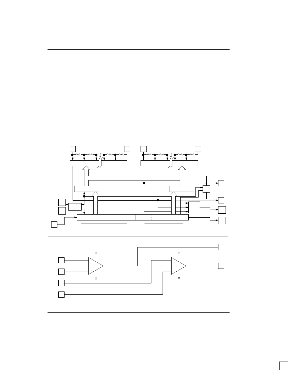
OPERATION - DIGITAL RESISTOR SECTION
The DS1667 contains two potentiometers, each of
which has its wiper set by a value contained in an 8 bit
register (see Figure 1). Each potentiometer consists of
256 resistors of equal value with tap points between
each resistor and at the low end.
In addition, the potentiometer can be stacked by con-
necting them in series such that the high end of poten-
tiometer 0 is connected to the low end of potentiometer
1. When stacking potentiometers, the stack select bit is
used to select which potentiometer wiper will appear at
the stack multiplexer output (SOUT). A zero written to
the stack multiplexer will connect wiper 0 to the SOUT
pin. This wiper will determine which of the 256 bottom
taps of the stacked potentiometer is selected. When a 1
is written to the stack multiplexer, wiper 1 is selected and
one of the upper 256 taps of the stacked potentiometer
is presented at the SOUT pin.
BLOCK DIAGRAM Figure 1
L0
H0
L1
H1
256–TO–1
MULTIPLEXER
256–TO–1
MULTIPLEXER
WIPER 0–8 BITS
WIPER 1–8 BITS
W1
W0
COUT
1 BIT
STACK SELECT
BIT
CONTROL
RST
CLK
DQ
I/O SHIFT REGISTER
RESISTOR SECTION
0
7
8
16
OP AMP SECTION
INV0
NINV0
INV1
NINV1
–
+
–
+
OUT0
OUT1
LOGIC
LSB
SS
WIPER0
MSB
WIPER1
MSB
LSB
STACK
MULTI–
PLEXER
SOUT
V
B
V
CC
V
B
V
CC