Rainbow Electronics DS1869 User Manual
Page 8
DS1869
8 of 8
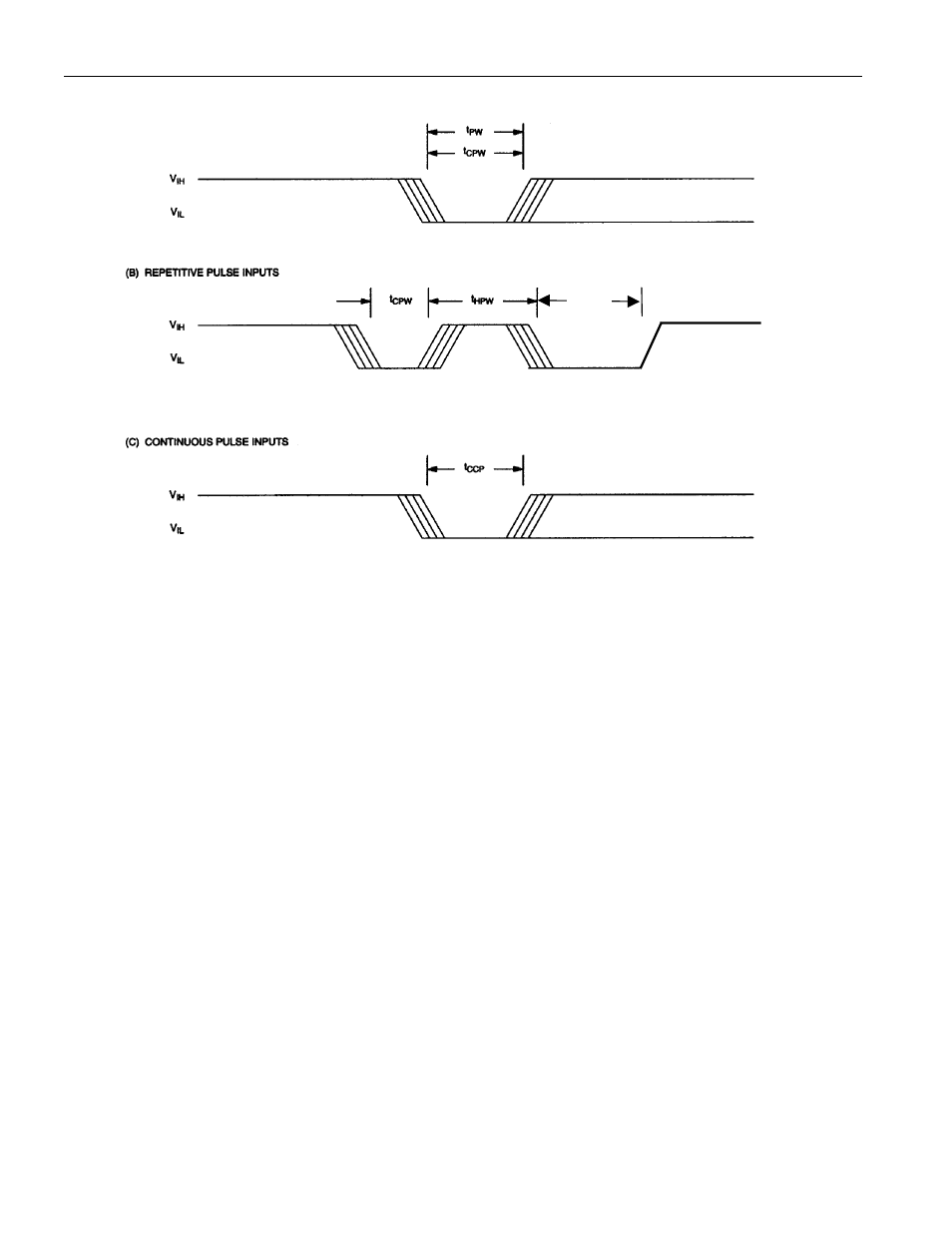
TIMING DIAGRAMS Figure 5
NOTES:
1. All inputs; UC, DC, and D are internally pulled up with a typical resistance of 100 k
Ω.
2. Input logic levels are referenced to -V.
3. I
CC
is the internal current that flows between -V and +V.
4. Input leakage applies to contact inputs UC and DC and the digital input (D).
5. Wiper current is the maximum current which can flow through the wipers.
6. Capacitance values apply at 25
°C.
7. Input pulse width is the minimum time required for an input to cause an increment or decrement. If
the UC, DC, or D input is held active for longer than 1 second, subsequent increments or decrements
will occur on 100 ms intervals until the inputs UC, DC, and/or D is released to V
IH
.
8. Repetitive pulsed inputs on UC, DC, or D will be recognized as long as the pulse repetition occurs
within 1 second of each other. Pulses occurring faster than 1 ms apart may not be recognized as
individual inputs but can be interpreted a constant input. Tolerance for pulse timing is
±15% on
minimum inputs.
9. Idle state supply current is measured with no pushbutton pressed and with the wiper R
W
tied to a
CMOS load.
10. For +V referenced to -V = 5V.
11. Valid at 25
°C only.
t
CPW