Rainbow Electronics DS12C887 User Manual
Page 14

DS12C887
14 of 19
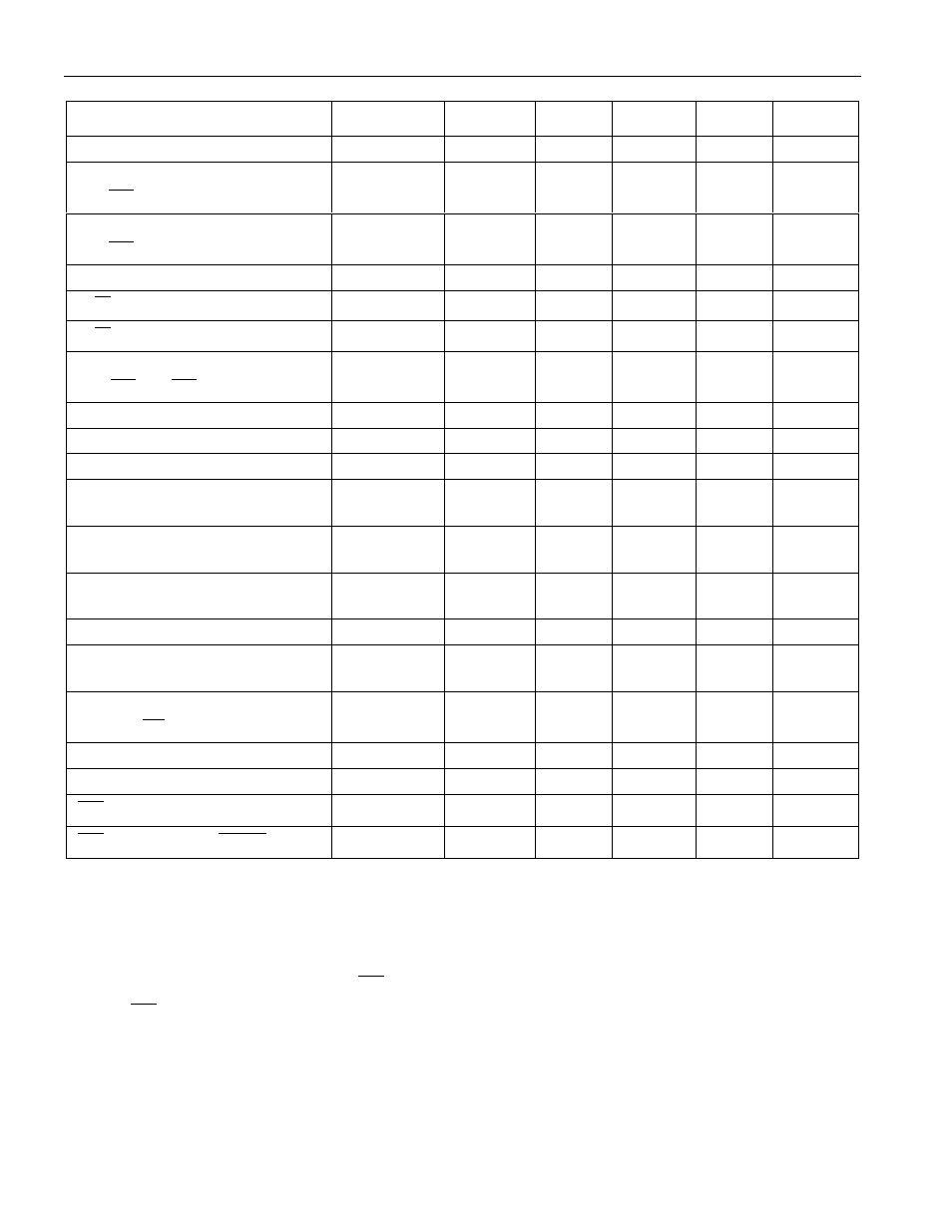
AC ELECTRICAL CHARACTERISTICS
(0°C to 70°C; VCC = 5.0V ± 10%)
PARAMETER
SYMBOL
MIN
TYP
MAX
UNITS
NOTES
Cycle Time
t
CYC
385
DC
ns
Pulse Width, DS/E Low or
RD/
WR
High
PW
EL
150
ns
Pulse Width, DS/E High or
RD/
WR
Low
PW
RH
125
ns
Input Rise and Fall
t
R
, t
F
30
ns
R/W Hold Time
t
RWH
10
ns
R/W Setup Time Before DS/E
t
RWS
50
ns
Chip Select Setup Time Before
DS,
WR
, or RD
t
CS
20
ns
Chip Select Hold Time
t
CH
0
ns
Read Data Hold Time
t
DHR
10
80
ns
Write Data Hold Time
t
DHW
0
ns
Mux’ed Address Valid Time to
ALE Fall
t
ASL
30
ns
Mused Address Hold Time to
ALE Fall
t
AHL
10
ns
Delay Time DS/E to AS/ALE
Rise
t
ASD
20
ns
Pulse Width AS/ALE High
PW
ASH
60
ns
Delay Time, AS/ALE to DS/E
Rise
t
ASED
40
ns
Output Data Delay Time from
DS/E or
RD
t
DDR
20
120
ns
6
Data Setup Time
t
DSW
100
ns
Reset Pulse Width
t
RWL
5
µ
s
IRQ
Release from DS
t
IRDS
2
µ
s
IRQ
Release from
RESET
t
IRR
2
µ
s
NOTES:
1. All voltages are referenced to ground.
2. All Outputs are open.
3. The MOT pin has an internal pull-down of 20K
Ω
.
4. Applies to the AD0-AD7 pins, the
IRQ
pin, and the SQW pin when each is in a high impedance state.
5. The
IRQ
pin is open drain.
6. Measured with a load as shown in Figure 4.
7. Real-Time Clock Modules can be successfully processed through conventional wave-soldering
techniques as long as temperature exposure to the lithium energy source contained within does not
exceed +85°C. Post solder cleaning with water washing techniques is acceptable, provided that
ultrasonic vibration is not used. Such cleaning can damage the crystal.
