Detailed description, Chip information, Package information – Rainbow Electronics DS4625 User Manual
Page 6: Pin configuration, Typical application circuit
DS4625
3.3V Dual-Output LVPECL Clock Oscillator
Maxim cannot assume responsibility for use of any circuitry other than circuitry entirely embodied in a Maxim product. No circuit patent licenses are
implied. Maxim reserves the right to change the circuitry and specifications without notice at any time.
6 _____________________Maxim Integrated Products, 120 San Gabriel Drive, Sunnyvale, CA 94086 408-737-7600
© 2009 Maxim Integrated Products
Maxim is a registered trademark of Maxim Integrated Products, Inc.
Detailed Description
The DS4625 is a dual-output, low-jitter clock oscillator
that produces frequency output pair combinations as
shown in the
Ordering Information/Selector Guide
table.
The phase relationship between the outputs is not guar-
anteed. The device combines an AT-cut, fundamental-
mode crystal, an oscillator, and a low-noise PLL in a
5.0mm x 3.2mm surface-mount LCCC package.
The DS4625 provides dual LVPECL clock output dri-
vers. The output drivers can be enabled and disabled
through the OE pin. The OE pin is an active-high CMOS
input that has an internal pullup resistor. When OE is
high, both output pairs are enabled.
Chip Information
PROCESS: Bipolar SiGe
Package Information
For the latest package outline information and land patterns, go
to
www.maxim-ic.com/packages
.
1
2
3
6
5
4
TOP VIEW
OE
GND
N.C.
N.C.
A1
A2
A3
A4
OP2
ON2
GND
V
CC
ON1
OP1
+
(5.00mm
× 3.20mm × 1.49mm)
DS4625
*EP
*EXPOSED PAD
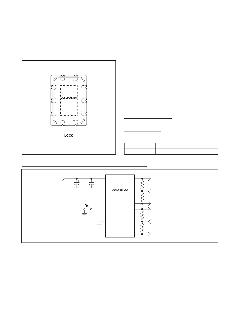
Pin Configuration
PACKAGE TYPE
PACKAGE CODE
DOCUMENT NO.
10 LCCC
L1053+H2
V
CC
OP1
ON1
OE
GND
0.01
μF
0.1
μF
50
Ω
50
Ω
PECL_BIAS AT V
CC
- 2.0V
OP2
ON2
50
Ω
50
Ω
PECL_BIAS AT V
CC
- 2.0V
DS4625
Typical Application Circuit