Single-sideband phase noise, Electrical characteristics (continued) – Rainbow Electronics DS4625 User Manual
Page 3

DS4625
3.3V Dual-Output LVPECL Clock Oscillator
_______________________________________________________________________________________
3
Note 2: Limits at -40°C are guaranteed by design and are not production tested.
Note 3: AC parameters are guaranteed by design and not production tested.
Note 4: Startup time is from V
CC
= V
CCMIN
until PLL locks to the crystal oscillator output.
Note 5: Frequency stability is calculated as:
Δf
TOTAL
=
Δf
TEMP
+
Δf
VCC
x (3.3 x 10%) +
Δf
LOAD
+
Δf
AGING
.
Note 6: Supply-induced jitter is the deterministic jitter as measured on a LeCroy SDA11000 measured with a 50mV
P-P
sine wave
forced on V
CC
.
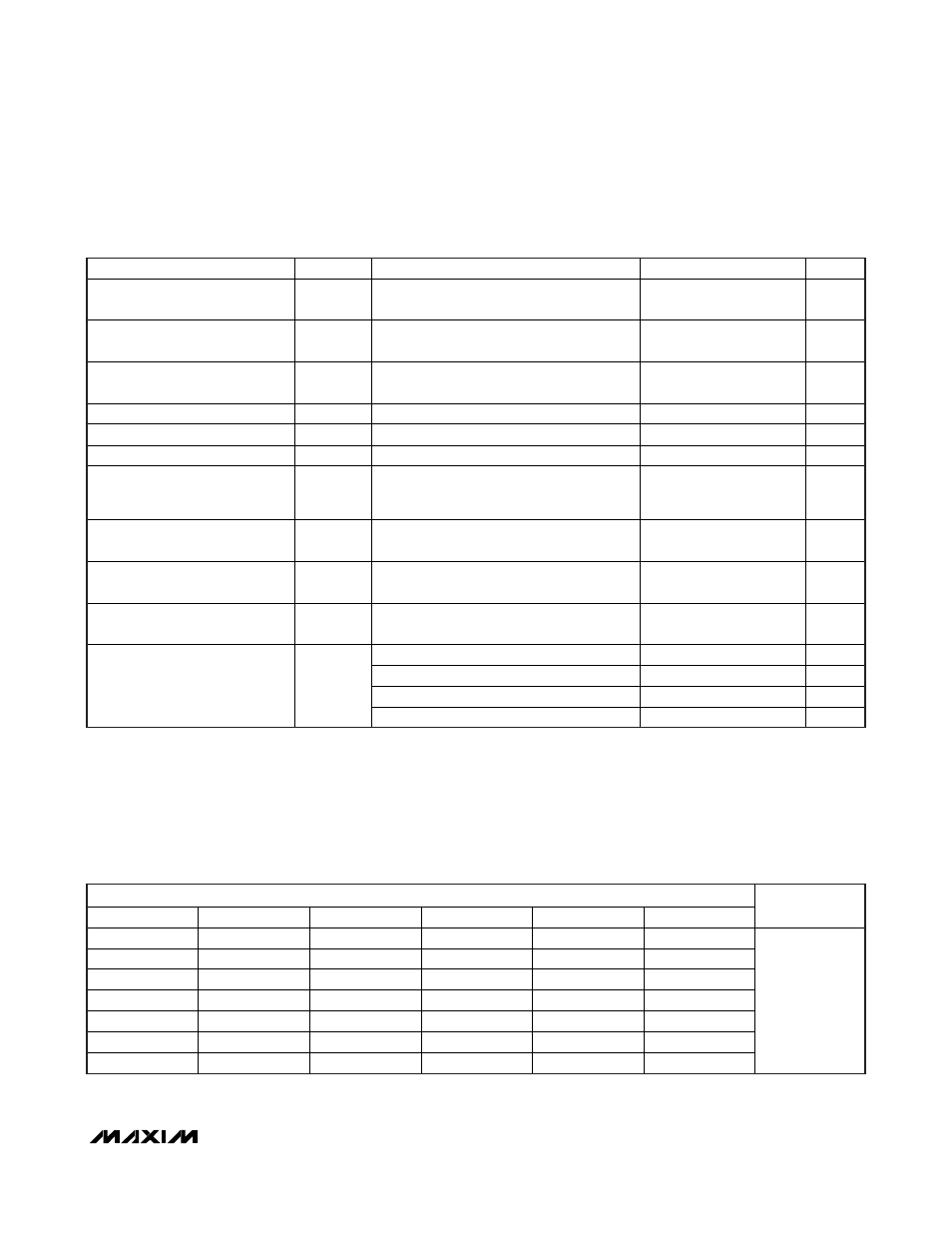
SINGLE-SIDEBAND PHASE NOISE
SSB PHASE NOISE (dBc/Hz) (TYPICAL, +25°C, +3.3V)
OFFSET f
C
= 100MHz
f
C
= 125MHz
f
C
= 150MHz
f
C
= 156.25MHz
f
C
= 200MHz
UNITS
100Hz
-71 -85 -84 -79 -85
1kHz -116 -117 -116 -115 -113
10kHz -119 -118 -116 -117 -113
100kHz
-126 -125 -122 -123 -120
1MHz -143 -142 -141 -140 -139
10MHz
-151 -149 -149 -148 -149
20MHz
-151 -150 -149 -149 -150
dBc/Hz
ELECTRICAL CHARACTERISTICS (continued)
(V
CC
= +2.97V to +3.63V, T
A
= -40°C to +70°C, typical values are at V
CC
= +3.3V and T
A
= +25°C, unless otherwise noted.) (Notes 2, 3)
PARAMETER SYMBOL
CONDITIONS
MIN
TYP
MAX
UNITS
Output High Voltage
V
OH
Output connected to 50
at PECL_BIAS at
V
CC
- 2.0V
V
CC
-
1.085
V
CC
-
0.88
V
Output Low Voltage
V
OL
Output connected to 50
at PECL_BIAS at
V
CC
- 2.0V
V
CC
-
1.825
V
CC
-
1.62
V
Differential Output Voltage
|V
OD
|
Output connected to 50
at PECL_BIAS at
V
CC
- 2.0V
0.595 0.710
V
Output Rise Time
t
R
20%
to
80%
200
ps
Output Fall Time
t
F
80%
to
20%
200 ps
Duty Cycle
D
CYCLE
45 55 %
Propagation Delay from OE
Going Low to Output High
Impedance
t
PAZ
(See Figure 2)
100
ns
Propagation Delay from OE
Going High to Output Active
t
PZA
(See Figure 2)
100
ns
Jitter J
RMS
Integrated phase RMS, 12kHz to 20MHz,
V
CC
= +3.3V, T
A
= +25°C
0.7 ps
Accumulated Deterministic
Jitter Due to Reference Spurs
125.00MHz output, V
CC
= +3.3V,
T
A
= +25°C
0.1
ps
10kHz
12.9
ps
100kHz
26.3
ps
200kHz
20.1
ps
Accumulated Deterministic
Jitter Due to Power-Supply Noise
(P-P) (Note 6)
1MHz
6.4
ps
