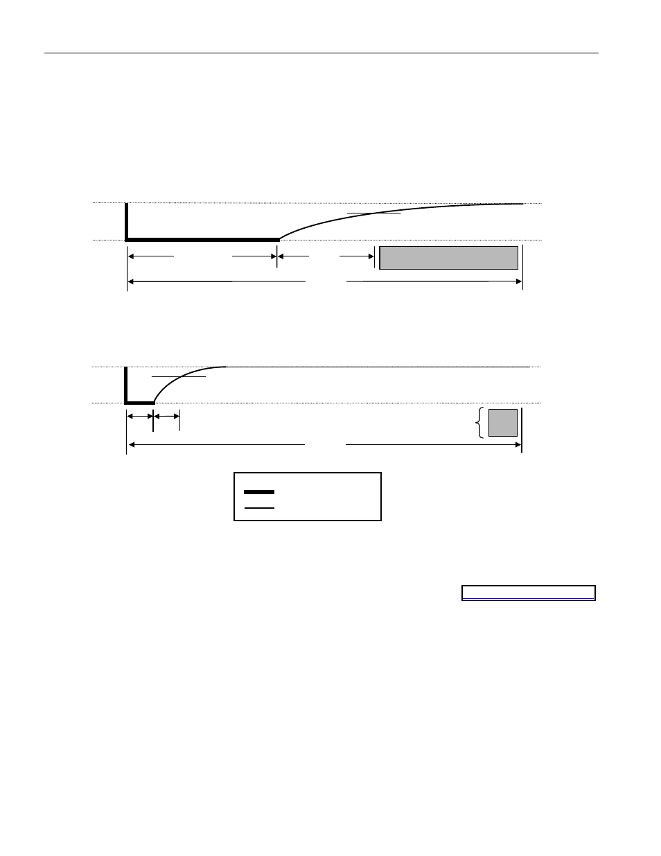
Detailed master read 1 timing figure 14, Recommended master read 1 timing figure 15, Related application notes – Rainbow Electronics DS18B20-PAR User Manual
Page 15: And t

DS18B20-PAR
15 of 19
the read time slot. Therefore, the master must release the bus and then sample the bus state within 15
µ
s
from the start of the slot.
Figure 14 illustrates that the sum of T
INIT
, T
RC
, and T
SAMPLE
must be less than 15
µ
s for a read time slot.
Figure 15 shows that system timing margin is maximized by keeping T
INIT
and T
RC
as short as possible
and by locating the master sample time during read time slots towards the end of the 15
µ
s period.
DETAILED MASTER READ 1 TIMING Figure 14
RECOMMENDED MASTER READ 1 TIMING Figure 15
RELATED APPLICATION NOTES
The following Application Notes can be applied to the DS18B20-PAR. These notes can be obtained from
the Dallas Semiconductor “Application Note Book,” via the Dallas website at
or through our faxback service at (214) 450–0441.
Application Note 27: “Understanding and Using Cyclic Redundancy Checks with Dallas Semiconductor
Touch Memory Product”
Application Note 55: “Extending the Contact Range of Touch Memories”
Application Note 74: “Reading and Writing Touch Memories via Serial Interfaces”
Application Note 104: “Minimalist Temperature Control Demo”
Application Note 106: “Complex MicroLANs”
Application Note 108: “MicroLAN – In the Long Run”
Sample 1-wire subroutines that can be used in conjunction with AN74 can be downloaded from the
Dallas website or anonymous FTP Site.
V
PU
GND
1-WIRE BUS
15
µµµµ
s
VIH of Master
T
RC
T
INT
> 1
µµµµ
s
Master samples
LINE TYPE LEGEND
Bus master pulling low
Resistor pullup
V
PU
GND
1-WIRE BUS
15
µµµµ
s
VIH of Master
T
RC
=
small
T
INT
=
small
Master samples
