Pin description, Isd2100 datasheet – Rainbow Electronics ISD2100 User Manual
Page 6
ISD2100 DATASHEET
Publication Release Feb 9, 2010
- 6 -
Revision 0.51
5
PIN DESCRIPTION
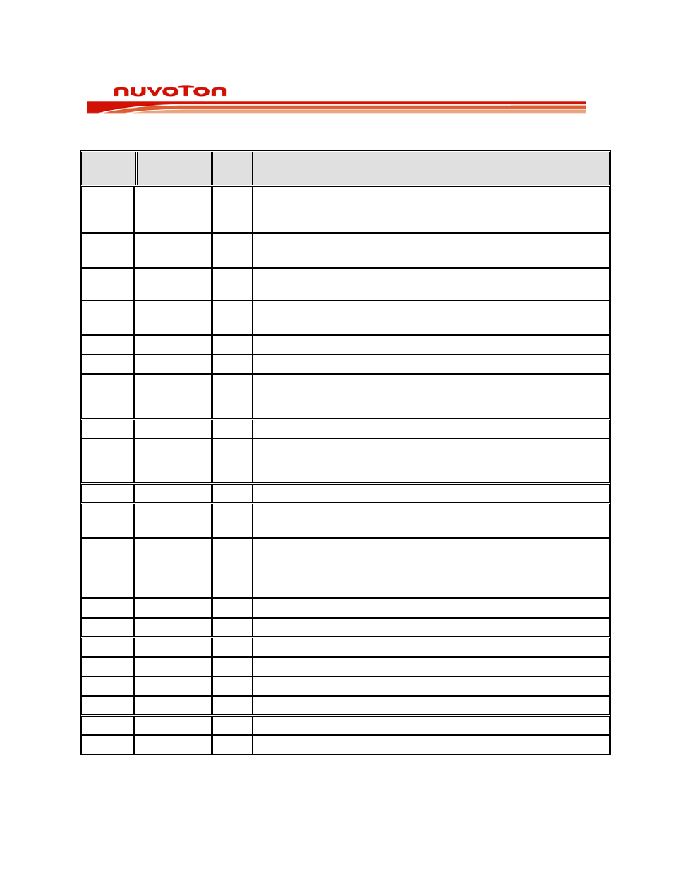
Pin
Number
Pin Name
I/O
Function
1
MISO /
GPIO2
O
Master-In-Slave-Out. Serial output from the ISD2100 to the host. This
pin is in tri-state when SSB=1.
Can be configured as a general purpose I/O pin.
2
SCLK / GPI1
I
Serial Clock input to the ISD2100 from the host.
Can be configured as a general purpose input pin.
3
SSB
I
Slave Select input to the ISD2100 from the host. When SSB is low
device is selected and responds to commands on the SPI interface.
4
MOSI /
GPIO0
I
Master-Out-Slave-In. Serial input to the ISD2100 from the host.
Can be configured as a general purpose I/O pin.
5
V
SSD
I
Digital Ground.
6
V
CCD
_PWM
I
Digital Power for the PWM Driver.
7
SPK+
O
PWM driver positive output. This SPK+ output, together with SPK- pin,
provide a differential output to drive 8
Ω speaker or buzzer. During
power down this pin is in tri-state.
8
V
SSD
_PWM
I
Digital Ground for the PWM Driver.
9
SPK-
O
PWM driver negative output. This SPK- output, together with SPK+
pin, provides a differential output to drive 8
Ω speaker or buzzer.
During power down this pin is tri-state.
10
V
CCD
_PWM
I
Digital Power for the PWM Driver.
11
INTB /
GPIO3
O
Active low interrupt request pin. This pin is an open-drain output.
Can be configured as a general purpose I/O pin.
12
RDY/BSYB /
GPIO4
O
An output pin to report the status of data transfer on the SPI interface.
“High” indicates that ISD2100 is ready to accept new SPI commands
or data.
Can be configured as a general purpose I/O pin.
13
NC
This pin should be left unconnected.
14
V
CCD
I
Digital Power.
15
GPIO5
I/O
General purpose I/O pin.
16
NC
This pin should be left unconnected.
17
NC
This pin should be left unconnected.
18
NC
This pin should be left unconnected.
19
NC
This pin should be left unconnected.
20
NC
This pin should be left unconnected.