Absolute maximum ratings, Operating ratings (notes , ), Converter electrical characteristics – Rainbow Electronics ADC12L063 User Manual
Page 5: Operating ratings
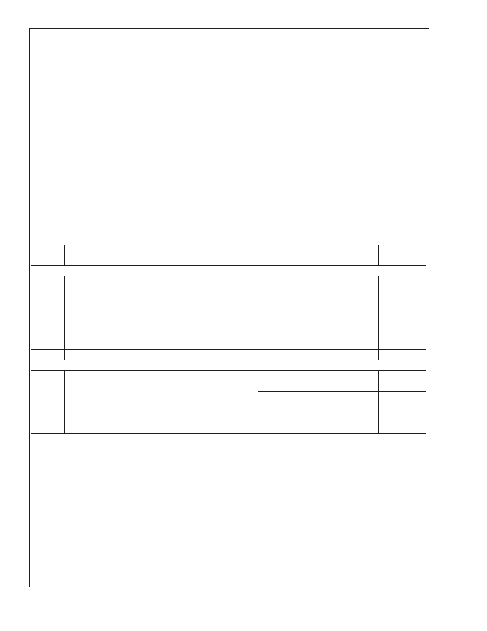
Absolute Maximum Ratings
(Notes 1,
If Military/Aerospace specified devices are required,
please contact the National Semiconductor Sales Office/
Distributors for availability and specifications.
V
A
, V
D
, V
DR
4.2V
|V
A
–V
D
|
≤ 100 mV
Voltage on Any Input or Output Pin
−0.3V to V
A
or V
D
+0.3V
Input Current at Any Pin (Note 3)
±
25 mA
Package Input Current (Note 3)
±
50 mA
Package Dissipation at T
A
= 25˚C
See (Note 4)
ESD Susceptibility
Human Body Model (Note 5)
2500V
Machine Model (Note 5)
250V
Soldering Temperature,
Infrared, 10 sec. (Note 6)
235˚C
Storage Temperature
−65˚C to +150˚C
Operating Ratings
(Notes 1, 2)
Operating Temperature
−40˚C
≤ T
A
≤ +85˚C
Supply Voltage (V
A
, V
D
)
+3.0V to +3.60V
Output Driver Supply (V
DR
)
+2.5V to V
D
V
REF
Input
0.8V to 1.2V
CLK, PD, OE
−0.05V to V
D
+ 0.05V
V
IN
Input
−0V to (V
A
− 0.5V)
|AGND–DGND|
≤100mV
Converter Electrical Characteristics
Unless otherwise specified, the following specifications apply for AGND = DGND = DR GND = 0V, V
A
= V
D
= V
DR
= +3.3V,
PD = 0V, V
REF
= +1.0V, f
CLK
= 62 MHz, t
r
= t
f
= 2 ns, C
L
= 20 pF/pin. Boldface limits apply for T
A
= T
J
= T
MIN
to T
MAX
: all
other limits T
A
= T
J
Symbol
Parameter
Conditions
Typical
Limits
Units
(Limits)
STATIC CONVERTER CHARACTERISTICS
Resolution with No Missing Codes
12
Bits
INL
Integral Non Linearity (Note 11)
±
1.0
±
2.4
LSB(max)
DNL
Differential Non Linearity
±
0.5
LSB(max)
GE
Gain Error
Positive Error
−0.8
%FS(max)
Negative Error
+0.1
±
3
%FS(max)
Offset Error (V
IN
+ = V
IN
−)
+0.1
±
0.9
%FS(max)
Under Range Output Code
0
0
Over Range Output Code
4095
4095
REFERENCE AND ANALOG INPUT CHARACTERISTICS
V
CM
Common Mode Input Voltage
1.0
V
C
IN
V
IN
Input Capacitance (each pin to
GND)
V
IN
= 1.0 Vdc
+ 1 V
P-P
(CLK LOW)
8
pF
(CLK HIGH)
7
pF
V
REF
Reference Voltage (Note 13)
1.00
0.8
V(min)
1.2
V(max)
Reference Input Resistance
100
M
Ω(min)
ADC12L063
www.national.com
5