Functional description, Applications information, 0 operating conditions – Rainbow Electronics ADC12L063 User Manual
Page 16: 1 analog inputs, 2 reference pins, 3 signal inputs, Figure 2. expected input signal range
Functional Description
Operating on a single +3.3V supply, the ADC12L063 uses a
pipelined architecture and has error correction circuitry to
help ensure maximum performance.
Differential analog input signals are digitized to 12 bits. Each
analog input signal should have a peak-to-peak voltage
equal to the input reference voltage, V
REF
, and be centered
around V
REF
/2. Table 1 and Table 2 indicate the input to the
output relationship of the ADC12L063. As indicated in Table
2, biasing one input to V
REF
/2 and driving the other input with
its full range signal results in a 6 dB reduction of the output
range, limiting it to the range of
1
⁄
4
to
3
⁄
4
of the minimum
output range obtainable if both inputs were driven with com-
plimentary signals. Section 1.3 explains how to avoid this
signal reduction.
TABLE 1. Input to Output Relationship —
Differential Input
V
IN+
V
IN−
Output
V
CM
−0.5
*
V
REF
V
CM
+0.5
*
V
REF
0000 0000 0000
V
CM
−0.25
*
V
REF
V
CM
+0.25
*
V
REF
0100 0000 0000
V
CM
V
CM
1000 0000 0000
V
CM
+0.25
*
V
REF
V
CM
−0.25
*
V
REF
1100 0000 0000
V
CM
+0.5
*
V
REF
V
CM
−0.5
*
V
REF
1111 1111 1111
TABLE 2. Input to Output Relationship —
Single-Ended Input
V
IN+
V
IN−
Output
V
CM
−V
REF
V
CM
0000 0000 0000
V
CM
−0.5
*
V
REF
V
CM
0100 0000 0000
V
CM
V
CM
1000 0000 0000
V
CM
+0.5
*
V
REF
V
CM
1100 0000 0000
V
CM
+V
REF
V
CM
1111 1111 1111
The output word rate is the same as the clock frequency,
which can be between 1 MSPS and 70 MSPS (typical). The
analog input voltage is acquired at the rising edge of the
clock and the digital data for that sample is delayed by the
pipeline for 6 clock cycles.
A logic high on the power down (PD) pin reduces the con-
verter power consumption to 50 mW.
Applications Information
1.0 OPERATING CONDITIONS
We recommend that the following conditions be observed for
operation of the ADC12L063:
3.0 V
≤ V
A
≤ 3.6V
V
D
= V
A
1.5V
≤ V
DR
≤ V
D
1 MHz
≤ f
CLK
≤ 70 MHz
0.8V
≤ V
REF
≤ 1.2V
1.1 Analog Inputs
The ADC12L063 has two analog signal inputs, V
IN+
and V
IN−
.
These two pins form a differential input pair. There is one
reference input pin, V
REF
.
1.2 Reference Pins
The ADC12L063 is designed to operate with a 1.0V refer-
ence, but performs well with reference voltages in the range
of 0.8V to 1.2V. Lower reference voltages will decrease the
signal-to-noise ratio (SNR) of the ADC12L063. Increasing
the reference voltage (and the input signal swing) beyond
1.2V will degrade THD for a full-scale input. It is very impor-
tant that all grounds associated with the reference voltage
and the input signal make connection to the analog ground
plane at a single point to minimize the effects of noise
currents in the ground path.
The three Reference Bypass Pins (V
RP
, V
RM
and V
RN
) are
made available for bypass purposes only. These pins should
each be bypassed to ground with a 0.1 µF capacitor. DO
NOT LOAD these pins.
1.3 Signal Inputs
The signal inputs are V
IN+
and V
IN−
. The input signal, V
IN
, is
defined as
V
IN
= (V
IN+
) – (V
IN−
)
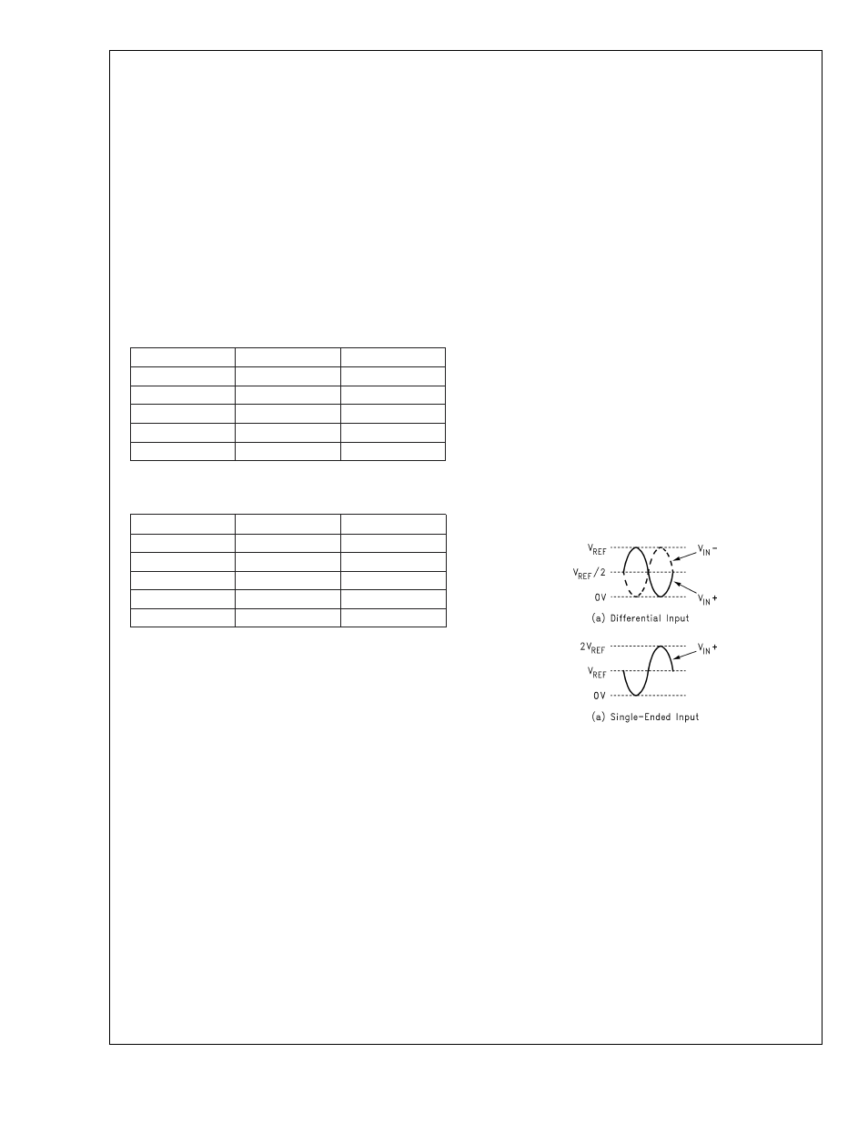
Figure 2 shows the expected input signal range.
Note that the nominal input common mode voltage, V
CM
, is
V
REF
/2, minimum and the nominal input signals each run
between the limits of AGND and 1.0V with V
REF
= 1.0V. If the
differential input signal increases above 2 V
P-P
, the minimum
input common mode voltage should increase proportionally.
The Peaks of the input signals should never exceed the
voltage described as
Peak Input Voltaged = V
A
− 1.0
to maintain dynamic performance.
The ADC12L063 performs best with a differential input with
each input centered around V
CM
(minimum of 0.5V). The
peak-to-peak voltage swing at both V
IN+
and V
IN−
should not
exceed the value of the reference voltage or the output data
will be clipped. The two input signals should be exactly 180˚
out of phase from each other and of the same amplitude. For
single frequency inputs, angular errors result in a reduction
of the effective full scale input. For a complex waveform,
however, angular errors will result in distortion.
For angular deviations of up to 10 degrees from these two
signals being 180 out of phase, the full scale error in LSB
can be described as approximately
E
FS
= dev
1.79
Where dev is the angular difference between the two signals
having a 180˚ relative phase relationship to each other (see
Figure 3). Drive the analog inputs with a source impedance
less than 100
Ω.
20026311
FIGURE 2. Expected Input Signal Range
ADC12L063
www.national.com
16