Figure 4, Applications information – Rainbow Electronics ADC12L063 User Manual
Page 18
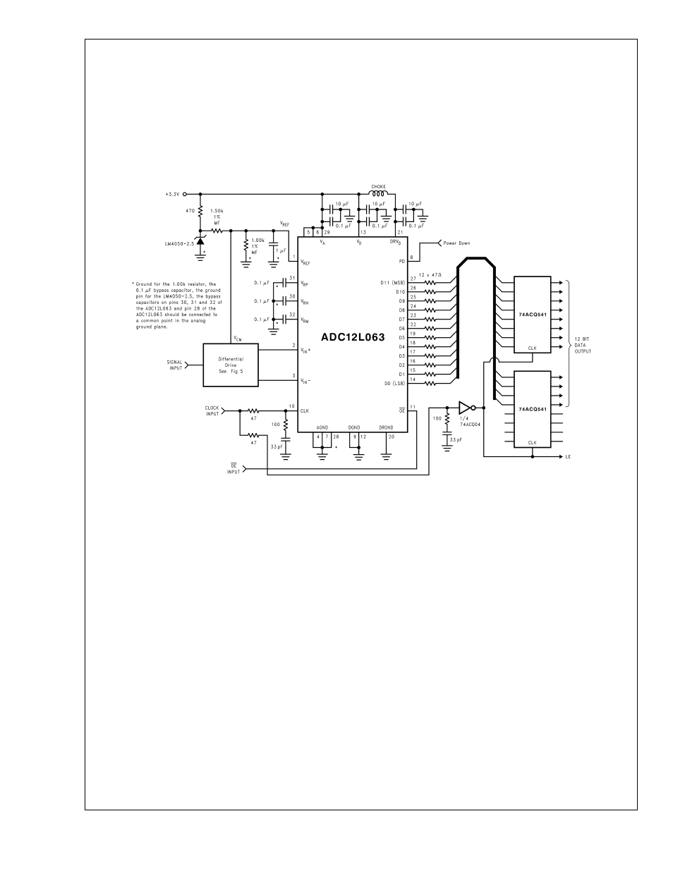
Applications Information
(Continued)
bypassing and careful attention to the ground plane will
reduce this problem. Additionally, bus capacitance beyond
the specified 20 pF/pin will cause t
OD
to increase, making it
difficult to properly latch the ADC output data. The result
could be an apparent reduction in dynamic performance.
To minimize noise due to output switching, minimize the load
currents at the digital outputs. This can be done by connect-
ing buffers between the ADC outputs and any other circuitry
(74ACQ541, for example). Only one input should be con-
nected to each output pin. Additionally, inserting series re-
sistors of 47
Ω to 56Ω at the digital outputs, close to the ADC
pins, will isolate the outputs from trace and other circuit
capacitances and limit the output currents, which could oth-
erwise result in performance degradation. See Figure 4.
While the ADC12L063 will operate with V
DR
voltages down
to 2.5V, t
OD
increases with reduced V
DR
. Be careful of
external timing when using reduced V
DR
.
20026313
FIGURE 4. Simple Application Circuit with Single-Ended to Differential Buffer
ADC12L063
www.national.com
18