Burst mode timing waveform – Rainbow Electronics DS17887 User Manual
Page 34
DS17885/DS17887
34 of 38
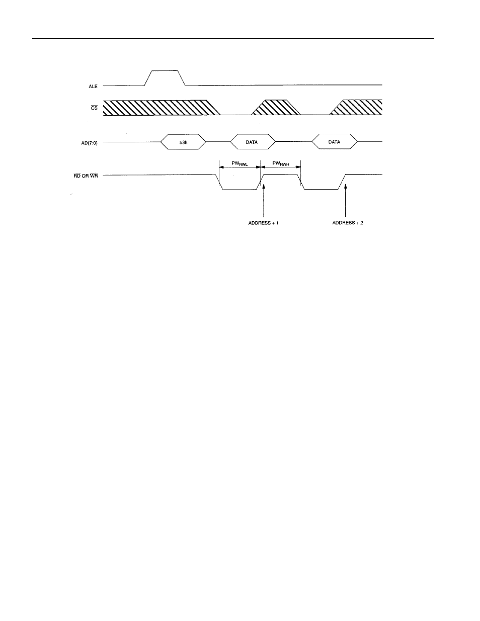
BURST MODE TIMING WAVEFORM
NOTES:
1) Typical values are at +25°C and nominal supplies.
2) Outputs are open.
3) Write-protection trip point occurs during power-fail prior to switchover from V
CC
to V
BAT
.
4) Applies to the AD0 to AD7 pins, and the SQW pin when each is in a high-impedance state.
5) The IRQ and PWR pins are open-drain.
6) Measured with a load of 50pF + 1 TTL gate.
7) Wake-up kickstart timeout generated only when the oscillator is enabled and the countdown chain is
not reset.
8) V
SW
is determined by the larger of V
BAT
and V
BAUX
.
9) The DS17887 keeps time to an accuracy of ±1 minute per month during data retention time for the
period of t
DR
.
10) t
DR
is the amount of time that the internal battery can power the internal oscillator and internal
registers of the DS17887.
11) I
BAT1
and I
BAT2
are measured at V
BAT
= 3.5V.
12) RTC modules can be successfully processed through conventional wave-soldering techniques as long
as temperature exposure to the lithium energy source contained within does not exceed +85°C. Post-
solder cleaning with water-washing techniques is acceptable, provided that ultrasonic vibration is not
used.