Note 3), Note 4), Note 5) – Rainbow Electronics ADC08200 User Manual
Page 6: Note 6), Note 9), Converter electrical characteristics
Converter Electrical Characteristics
(Continued)
The following specifications apply for V
A
= V
DR
= +3.0V
DC
, V
RT
= +1.9V, V
RB
= 0.3V, C
L
= 5 pF, f
CLK
= 200 MHz at 50% duty
cycle. Boldface limits apply for T
J
= T
MIN
to T
MAX
: all other limits T
J
= 25˚C (Notes 7, 8)
Symbol
Parameter
Conditions
Typical
Limits
Units
(Limits)
POWER SUPPLY CHARACTERISTICS
I
DR
Output Driver Supply Current
DC Input, PD = Low
0.25
0.6
mA (max)
I
A
+ I
DR
Total Operating Current
DC Input, PD = Low
70
86.6
mA (max)
CLK Low, PD = Hi
0.3
mA
PC
Power Consumption
DC Input, Excluding Reference
210
260
mW (max)
CLK Low, PD = Hi
1
mW
PSRR
1
Power Supply Rejection Ratio
FSE change with 2.7V to 3.3V change
in V
A
54
dB
PSRR
2
Power Supply Rejection Ratio
SNR reduction with 200 mV at 1MHz
on supply
45
dB
AC ELECTRICAL CHARACTERISTICS
f
C1
Maximum Conversion Rate
230
200
MHz (min)
f
C2
Minimum Conversion Rate
10
MHz
t
CL
Minimum Clock Low Time
0.87
1.0
ns (min)
t
CH
Minimum Clock High Time
0.65
0.75
ns (min)
t
OH
Output Hold Time
CLK to Data Invalid
2.1
ns
t
OD
Output Delay
CLK to Data Transition
3.5
2.5
ns (min)
5
ns (max)
Pipeline Delay (Latency)
6
Clock Cycles
t
AD
Sampling (Aperture) Delay
CLK Rise to Acquisition of Data
2.6
ns
t
AJ
Aperture Jitter
2
ps rms
Note 1: Absolute Maximum Ratings indicate limits beyond which damage to the device may occur. Operating Ratings indicate conditions for which the device is
functional, but do not guarantee specific performance limits. For guaranteed specifications and test conditions, see the Electrical Characteristics. The guaranteed
specifications apply only for the test conditions listed. Some performance characteristics may degrade when the device is not operated under the listed test
conditions.
Note 2: All voltages are measured with respect to GND = AGND = DR GND = 0V, unless otherwise specified.
Note 3: When the input voltage at any pin exceeds the power supplies (that is, less than AGND or DR GND, or greater than V
A
or V
DR
), the current at that pin should
be limited to 25 mA. The 50 mA maximum package input current rating limits the number of pins that can safely exceed the power supplies with an input current of
25 mA to two.
Note 4: The absolute maximum junction temperature (T
J
max) for this device is 150˚C. The maximum allowable power dissipation is dictated by T
J
max, the
junction-to-ambient thermal resistance (
θ
JA
), and the ambient temperature (T
A
), and can be calculated using the formula P
D
MAX = (T
J
max − T
A
) /
θ
JA
. The values
for maximum power dissipation listed above will be reached only when this device is operated in a severe fault condition (e.g., when input or output pins are driven
beyond the power supply voltages, or the power supply polarity is reversed). Obviously, such conditions should always be avoided.
Note 5: Human body model is 100 pF capacitor discharged through a 1.5 k
Ω resistor. Machine model is 220 pF discharged through ZERO Ohms.
Note 6: See AN-450, “Surface Mounting Methods and Their Effect on Product Reliability”.
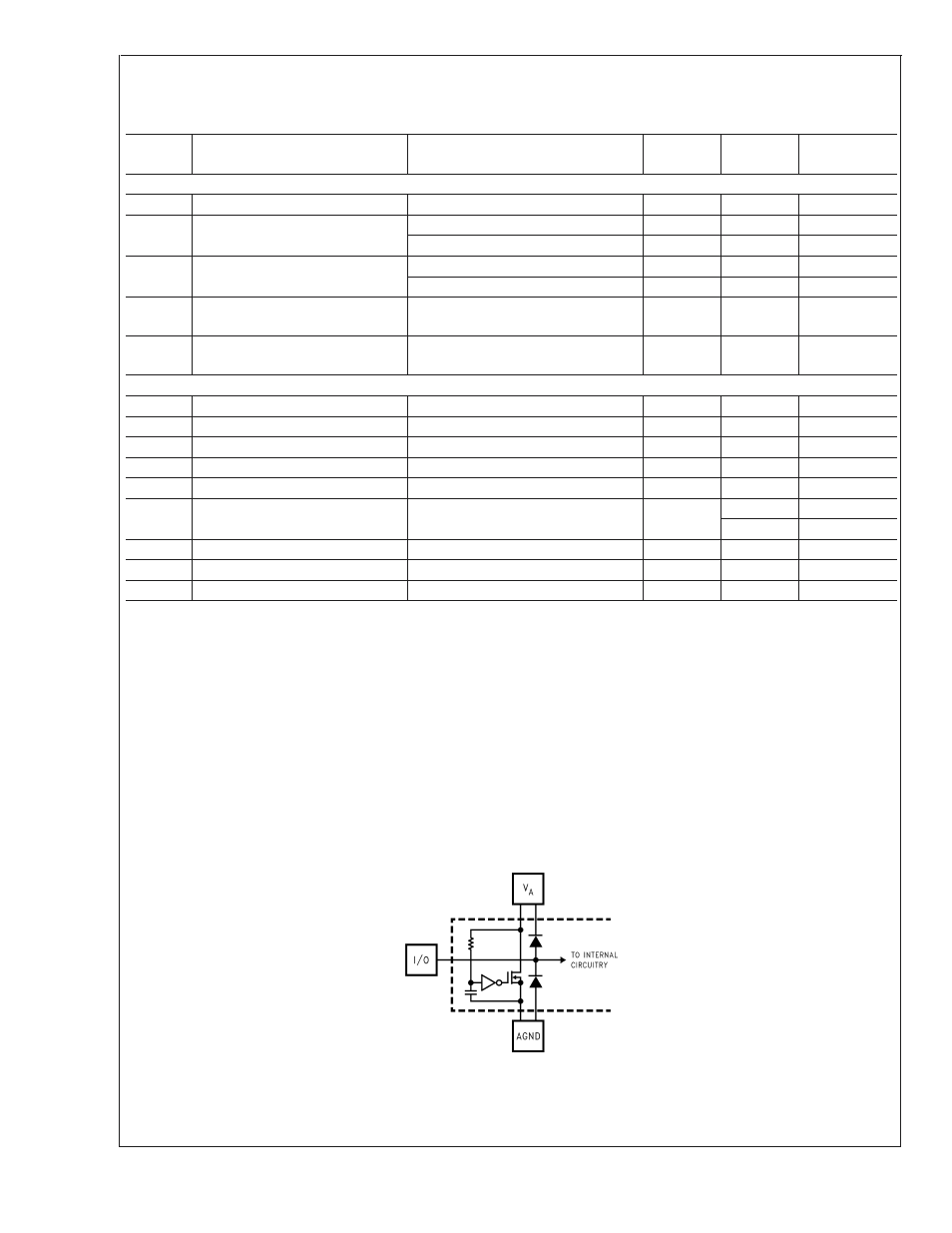
Note 7: The analog inputs are protected as shown below. Input voltage magnitudes up to V
A
+ 300 mV or to 300 mV below GND will not damage this device.
However, errors in the A/D conversion can occur if the input goes above V
DR
or below GND by more than 100 mV. For example, if V
A
is 2.7V
DC
the full-scale input
voltage must be
≤2.8V
DC
to ensure accurate conversions.
20017907
Note 8: To guarantee accuracy, it is required that V
A
and V
DR
be well bypassed. Each supply pin must be decoupled with separate bypass capacitors.
Note 9: Typical figures are at T
J
= 25˚C, and represent most likely parametric norms. Test limits are guaranteed to National’s AOQL (Average Outgoing Quality
Level).
ADC08200
www.national.com
6