0 layout and grounding, Figure 5. layout example, 0 dynamic performance – Rainbow Electronics ADC08200 User Manual
Page 16: 0 common application pitfalls, Applications information
Applications Information
(Continued)
The CLOCK line should be series terminated at the clock
source in the characteristic impedance of that line if the clock
line is longer than
where t
r
is the clock rise time and t
prop
is the propagation rate
of the signal along the trace. Typical t
prop
is about 150
ps/inch (59 ps/cm) on FR-4 board material.
If the clock source is used to drive more than just the
ADD08200, the CLOCK pin should be a.c. terminated with a
series RC to ground such that the resistor value is equal to
the characteristic impedance of the clock line and the ca-
pacitor value is
where t
PD
is the signal propagation rate down the clock line,
"L" is the line length and Z
O
is the characteristic impedance
of the clock line. This termination should be located as close
as possible to, but within one centimeter of, the ADC08200
clock pin. Further, this termination should be close to but
beyond the ADC08200 clock pin as seen from the clock
source. Typical t
prop
is about 150 ps/inch on FR-4 board
material. For FR-4 board material, the value of C becomes
Where L is the length of the clock line in inches.
This termination should be located as close as possible to,
but within one centimeter of, the ADC08200 clock pin.
5.0 LAYOUT AND GROUNDING
Proper grounding and proper routing of all signals are es-
sential to ensure accurate conversion. A combined analog
and digital ground plane should be used.
Since digital switching transients are composed largely of
high frequency components, total ground plane copper
weight will have little effect upon the logic-generated noise
because of the skin effect. Total surface area is more impor-
tant than is total ground plane volume. Capacitive coupling
between the typically noisy digital circuitry and the sensitive
analog circuitry can lead to poor performance that may seem
impossible to isolate and remedy. The solution is to keep the
analog circuitry well separated from the digital circuitry.
High power digital components should not be located on or
near a straight line between the ADC or any linear compo-
nent and the power supply area as the resulting common
return current path could cause fluctuation in the analog
input “ground” return of the ADC.
Generally, analog and digital lines should cross each other at
90˚ to avoid getting digital noise into the analog path. In high
frequency systems, however, avoid crossing analog and
digital lines altogether. Clock lines should be isolated from
ALL other lines, analog AND digital. Even the generally
accepted 90˚ crossing should be avoided as even a little
coupling can cause problems at high frequencies. Best per-
formance at high frequencies is obtained with a straight
signal path.
The analog input should be isolated from noisy signal traces
to avoid coupling of spurious signals into the input. Any
external component (e.g., a filter capacitor) connected be-
tween the converter’s input and ground should be connected
to a very clean point in the analog ground plane.
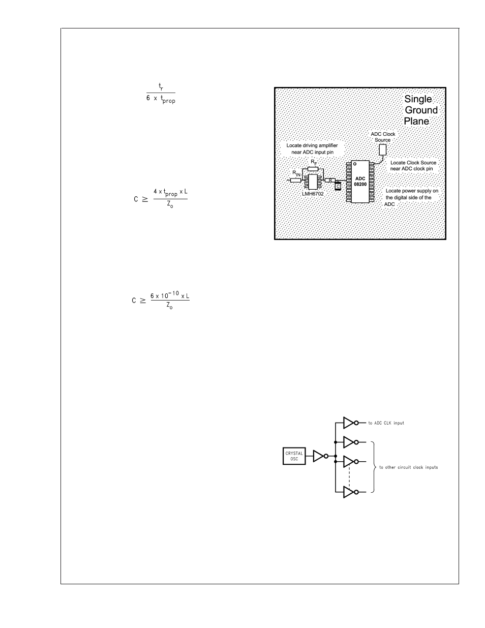
Figure 5 gives an example of a suitable layout. All analog
circuitry (input amplifiers, filters, reference components, etc.)
should be placed together away from any digital compo-
nents.
6.0 DYNAMIC PERFORMANCE
The ADC08200 is a.c. tested and its dynamic performance is
guaranteed. To meet the published specifications, the clock
source driving the CLK input must exhibit less than 2 ps
(rms) of jitter. For best a.c. performance, isolating the ADC
clock from any digital circuitry should be done with adequate
buffers, as with a clock tree. See Figure 6.
It is good practice to keep the ADC clock line as short as
possible and to keep it well away from any other signals.
Other signals can introduce jitter into the clock signal. The
clock signal can also introduce noise into the analog path.
7.0 COMMON APPLICATION PITFALLS
Driving the inputs (analog or digital) beyond the power
supply rails. For proper operation, all inputs should not go
more than 300 mV below the ground pins or 300 mV above
20017936
FIGURE 5. Layout Example
20017937
FIGURE 6. Isolating the ADC Clock from Digital
Circuitry
ADC08200
www.national.com
16