Ordering information, Block diagram, Pin descriptions and equivalent circuits – Rainbow Electronics ADC08200 User Manual
Page 2
Ordering Information
Order Number (−40˚C
≤ T
A
≤ +85˚C)
Package
ADC08200CIMT
TSSOP
ADC08200CIMTX
TSSOP (tape and reel)
ADC08200EVAL
Evaluation Board
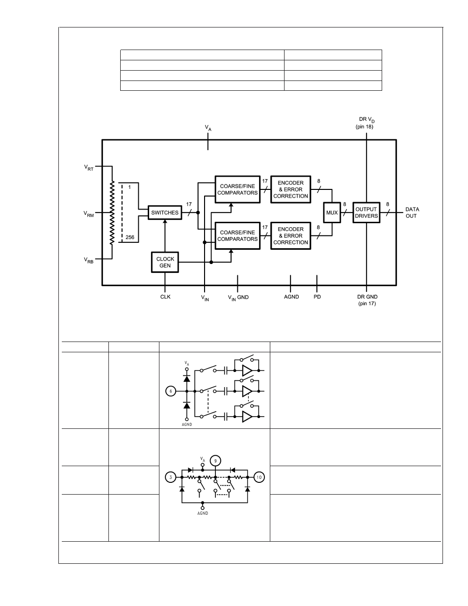
Block Diagram
20017902
Pin Descriptions and Equivalent Circuits
Pin No.
Symbol
Equivalent Circuit
Description
6
V
IN
Analog signal input. Conversion range is V
RB
to V
RT
.
3
V
RT
Analog Input that is the high (top) side of the reference
ladder of the ADC. Nominal range is 0.5V to V
A
. Voltage
on V
RT
and V
RB
inputs define the V
IN
conversion range.
Bypass well. See Section 2.0 for more information.
9
V
RM
Mid-point of the reference ladder. This pin should be
bypassed to a quiet point in the analog ground plane with
a 0.1 µF capacitor.
10
V
RB
Analog Input that is the low side (bottom) of the
reference ladder of the ADC. Nominal range is 0.0V to
(V
RT
– 0.5V). Voltage on V
RT
and V
RB
inputs define the
V
IN
conversion range. Bypass well. See Section 2.0 for
more information.
ADC08200
www.national.com
2