I/o shift register figure 3, Stacked configuration, Stacked configuration figure 4 cascade operation – Rainbow Electronics DS1867 User Manual
Page 5
DS1867
5 of 14
102199
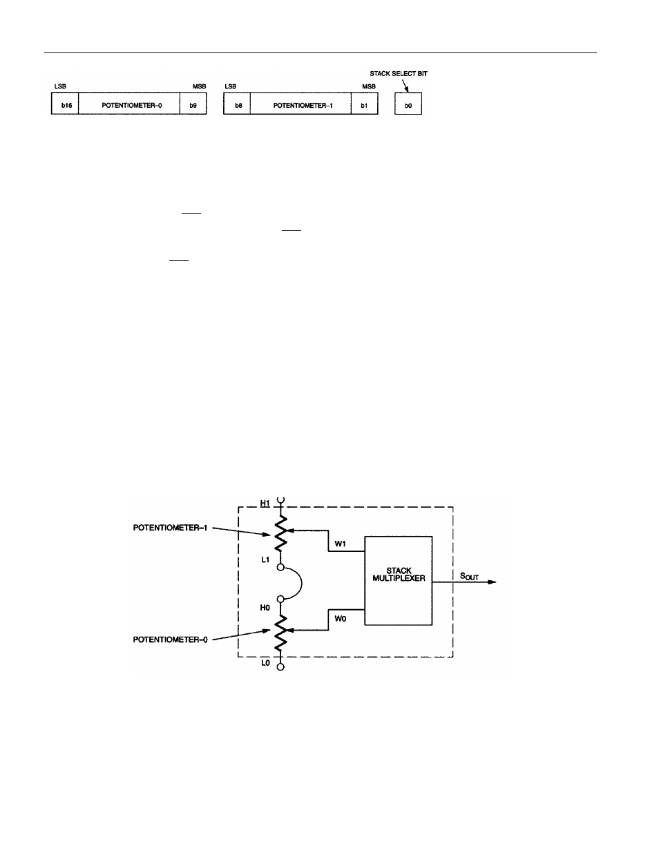
I/O SHIFT REGISTER Figure 3
17-BIT I/O SHIFT REGISTER
Transmission of data always begins with the stack select bit followed by the potentiometer-1 wiper
position value and lastly the potentiometer-0 wiper position value (see Figure 2(a)).
When wiper position data is to be written to the DS1867, 17-bits (or some integer multiple) of data should
always be transmitted. Transactions which do not send a complete 17-bits (or multiple) will leave the
register incomplete and possibly an error in desired wiper position. After a communication transaction
has been completed the
RST
signal input should be taken to a low state to prevent any inadvertent
changes to the device shift register. Once
RST
has reached a low state, the contents of the I/O shift
register are loaded into the respective multiplexers for setting wiper position. A new wiper position will
only engage pending a
RST
transition to the low state. The wiper position for the high-end terminals H0
and H1 will have data values FF (hex), while the low-end terminals will have data values 00 (hex).
STACKED CONFIGURATION
The potentiometers of the DS1867 can be connected in series as shown in Figure 4. This is referred to as
the stacked configuration and allows the user to double the total end-to-end resistance of the part. The
resolution of the combined potentiometers will remain the same as a single potentiometer but with a total
of 512 wiper positions available. Device resolution is defined as R
TOT
/256 (per potentiometer); where
R
TOT
is equal to the device resistance value. The wiper output for the combined stacked potentiometer will
be taken at the S
out
pin, which is the multiplexed output of the wiper of potentiometer-0 (W0) or
potentiometer-1 (W1). The potentiometer wiper selected at the S
out
output is governed by the setting of
the stack select bit (bit-0) of the 17-bit I/O shift register. If the stack select bit has value 0, the multiplexed
output, S
out
, will be that of the potentiometer-0 wiper. If the stack select bit has value 1, the multiplexed
output, S
out
, will be that of the potentiometer-1 wiper.
STACKED CONFIGURATION Figure 4
CASCADE OPERATION
A feature of the DS1867 is the ability to control multiple devices from a single processor. Multiple
DS1867s can be linked or daisy-chained as shown in Figure 5. As a data bit is entered into the I/O shift
register of the DS1867 it will appear at the C
out
output after a maximum delay of 70 nanoseconds.