Rainbow Electronics BA4510FV User Manual
Page 3
3
Standard ICs
BA4510F / BA4510FV
•
Electrical characteristics (unless otherwise noted, Ta = 25°C, V
CC
= ±2.5V)
Parameter
Symbol
Min.
Typ.
Max.
Unit
Input offset voltage
V
IO
—
1
6
mV
R
S
= 50
Ω
Input offset current
I
IO
—
2
200
nA
Input bias current
I
B
—
80
500
nA
High-amplitude voltage gain
A
V
60
90
—
dB
Common-mode input voltage
V
ICM
– 1.3
—
V
Common-mode rejection ratio
CMRR
60
80
—
dB
Power supply voltage rejection ratio
PSRR
60
80
—
dB
R
S
= 50
Ω
Quiescent current
I
Q
2.5
5.0
7.5
mA
Output voltage
High
V
OH
2.0
2.4
—
V
R
L
= 2k
Ω
Low
V
OL
—
– 2.4
– 2.0
V
R
L
= 2k
Ω
Slew rate
S.R.
5
V /
µ
s
—
1.5
—
Conditions
R
L
м
2k
Ω
, V
CC
= 15V
R
L
=
∞
ALL AMPS
∗
1
∗
1 Because the first stage is configured with a PNP transistor, input bias current is from the IC.
•
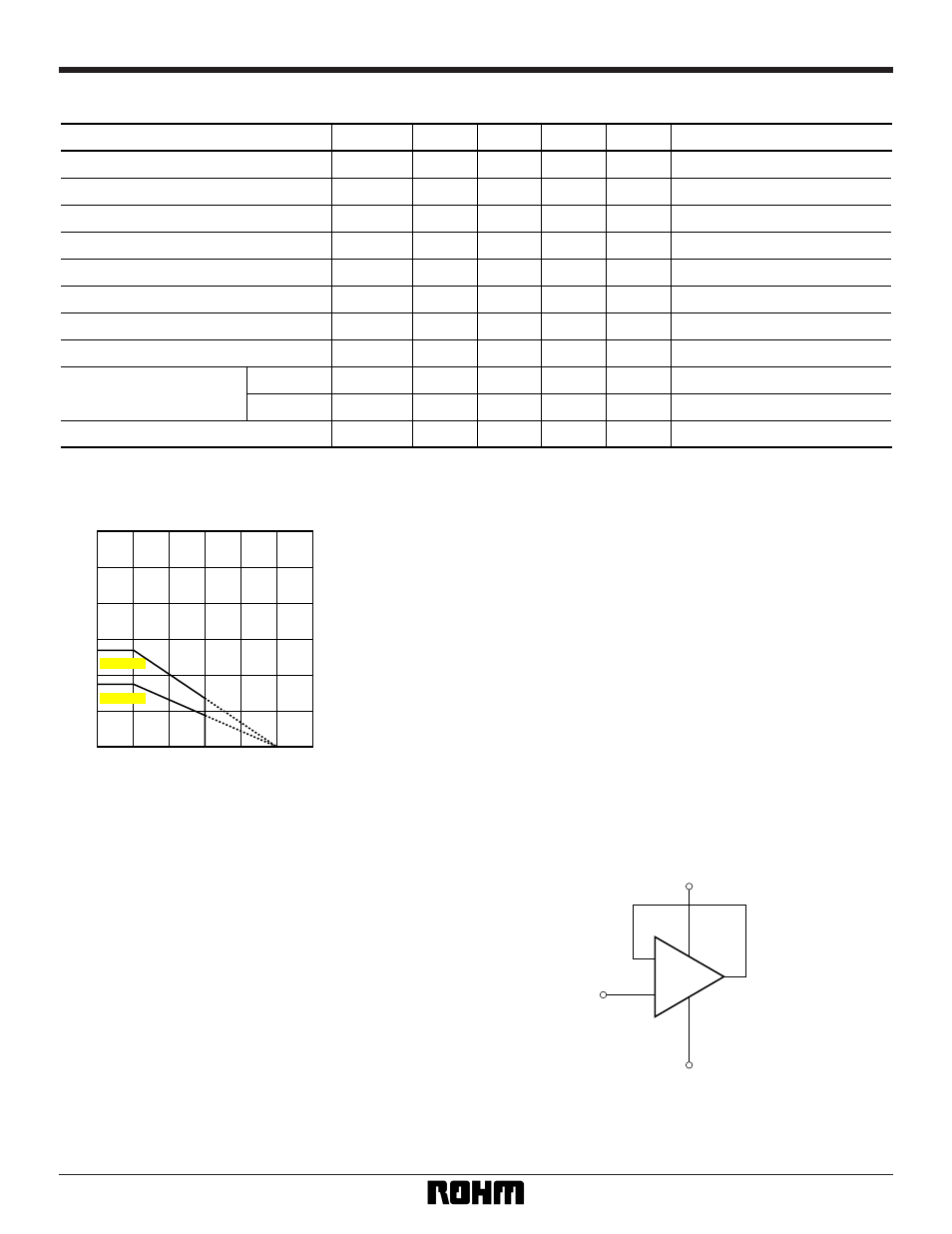
Electrical characteristic curve
POWER DISSIPATION: Pd (mW)
AMBIENT TEMPERATURE: Ta (
°
C)
1200
1000
800
600
400
200
0
0
25
50
75
100
125
150
BA4510F
BA4510FV
Fig. 1 Power dissipation vs. ambient
temperature
•
Operation notes
(1) Unused circuit connections
If there are any circuits which are not being used, we
recommend making connections as shown in Figure 2,
with the non-inverted input pin connected to the poten-
tial within the in-phase input voltage range (V
ICM
).
(2) If used with a voltage follower, be careful of oscilla-
tion which may cause problems with the in-line input
voltage range or the capacitance load.
(3) If using at power supply voltage + 5.0 or higher, be
sure the gain is reduced sufficiently to prevent oscilla-
tion.
V
CC
V
EE
To potential
in V
ICM
+
–
Fig. 2 Unused circuit connections