Electrical characteristics (continued) – Rainbow Electronics ATR0635P1 User Manual
Page 30
30
4979D–GPS–06/08
ATR0635P1
6.7
Schmitt trigger hysteresis
VDD18 = 1.65V to 1.95V
CLK23
V
hyst,CLK23
0.2
0.55
V
C
6.8
Schmitt trigger threshold
rising
VDD18 = 1.65V to 1.95V
NRESET V
th+,NRESET
0.8
1.3
V
C
6.9
Schmitt trigger threshold
falling
VDD18 = 1.65V to 1.95V
NRESET
V
th-,NRESET
0.46
0.77
V
C
6.10
Low-level input voltage
VDDIO domain
VDDIO = 1.65V to 3.6V
V
IL,IO
–0.3
+0.41
V
C
6.11
High-level input voltage
VDDIO domain
VDDIO = 1.65V to 3.6V
V
IH,IO
1.46
5.0
V
C
6.12
Low-level input voltage
VBAT18 domain
VBAT18 = 1.65V to 1.95V
A11, B10,
C10, D10
V
IL,BAT
–0.3
+0.41
V
C
6.13
High-level input voltage
VBAT18 domain
VBAT18 = 1.65V to 1.95V
A11, B10,
C10, D10
V
IH,BAT
1.46
5.0
V
C
6.14 Low-level input voltage USB VDD_USB = 3.0V to 3.6V
C9, D9
V
IL,USB
–0.3
+0.8
V
C
6.15
High-level input voltage
USB
VDD_USB = 3.0V to 3.6V
39
Ω
source resistance +
27
Ω
external series resistor
C9, D9
V
IH,USB
2.0
4.6
V
C
6.16
Low-level output voltage
VDD18 domain
I
OL
= 1.5 mA,
VDD18 = 1.65V
V
OL,18
0.4
V
A
6.17
High-level output voltage
VDD18 domain
I
OH
= –1.5 mA,
VDD18 = 1.65V
V
OH,18
VDD18
– 0.45
V
A
6.18
Low-level output voltage
VDDIO domain
I
OL
= 1.5 mA,
VDDIO = 3.0V
V
OL,IO
0.4
V
A
6.19
High-level output voltage
VDDIO domain
I
OH
= –1.5 mA,
VDDIO = 3.0V
V
OH,IO
VDDIO
– 0.5
V
A
6.20
Low-level output voltage
VBAT18 domain
I
OL
= 1 mA
P9, P13,
P22, P31
V
OL,BAT
0.4
V
A
6.21
High-level output voltage
VBAT18 domain
I
OH
= –1 mA
P9, P13,
P22, P31
V
OH,BAT
1.2
V
A
6.22
Low-level output voltage
USB
I
OL
= 2.2 mA,
VDD_USB = 3.0V to 3.6V,
27
Ω
external series resistor
DP, DM
V
OL,USB
0.3
V
A
6.23
High-level output voltage
USB
I
OH
= 0.2 mA,
VDD_USB = 3.0V to 3.6V,
27
Ω
external series resistor
DP, DM
V
OH,USB
2.8
V
A
6.24
Input-leakage current
(standard inputs and I/Os)
VDD18 = 1.95V
V
IL
= 0V
I
LEAK
–1
+1
µA
C
6.25 Input capacitance
I
CAP
10
pF
D
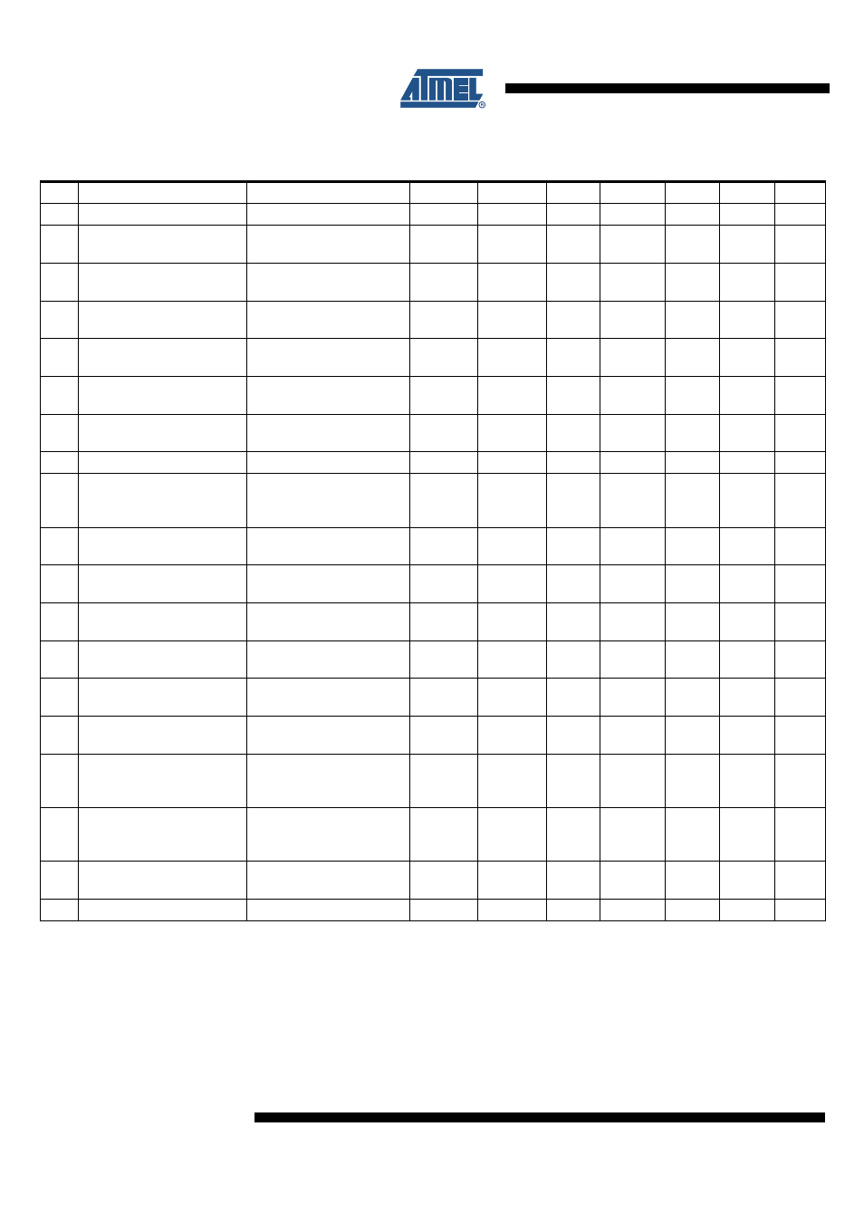
10. Electrical Characteristics (Continued)
If no additional information is given in column Test Conditions, the values apply to temperature range from –40°C to +85°C.
No. Parameters
Test Conditions
Pin
Symbol
Min
Typ
Max
Unit
Type*
*) Type means: A = 100% tested, B = 100% correlation tested, C = Characterized on samples, D = Design parameter
Notes:
1. The LDO18 is a built in low dropout voltage regulator, which can be used if the host system does not provide the core volt-
age VDD18.
2. The LDOBAT is a built in low dropout voltage regulator, which provides the supply voltage VBAT18 for the RTC, backup
SRAM, P9, P13, P22, P31, NSLEEP and NSHDN. The LDOBAT voltage regulator switches in battery mode if LDOBAT_IN
falls below 1.5V.
3. Supply voltage VBAT18 for backup domain is generated internally by the LDOBAT.
4. If no current is caused by outputs (pad output current as well as current across internal pull-up resistors)