Rainbow Electronics DS1267 User Manual
Page 3

DS1267
3 of 12
102199
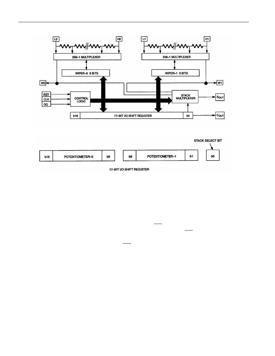
DS1267 BLOCK DIAGRAM Figure 1
I/O SHIFT REGISTER Figure 2
Transmission of data always begins with the stack select bit followed by the potentiometer-1 wiper
position value and lastly the potentiometer-0 wiper position value.
When wiper position data is to be written to the DS1267, 17 bits (or some integer multiple) of data should
always be transmitted. Transactions which do not send a complete 17-bits (or multiple) will leave the
register incomplete and possibly an error in the desired wiper positions.
After a communication transaction has been completed, the
RST
signal input should be taken to a low
state to prevent any inadvertent changes to the device shift register. Once
RST
has reached a low state,
the contents of the I/O shift register are loaded into the respective multiplexers for setting wiper position.
A new wiper position will only engage after a
RST
transition to the inactive state. On device power-up
the DS1267 wiper positions will be set at 50% of the total resistance or binary value 1000 0000.
