Note 3), Note 4), Note 5) – Rainbow Electronics ADC10321 User Manual
Page 7: Note 6), 25˚c(note 7), Ac electrical characteristics
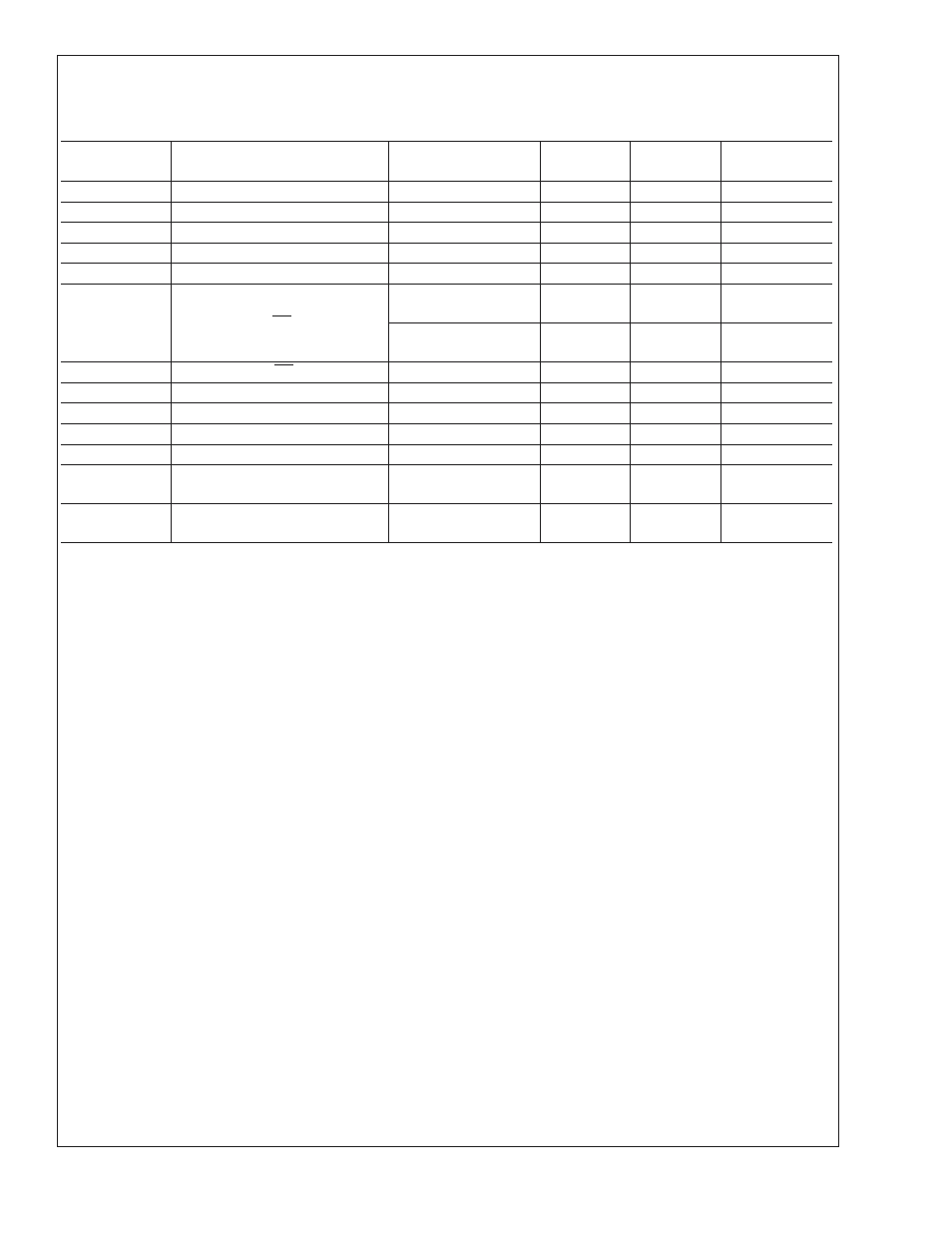
AC Electrical Characteristics
(Continued)
The following specifications apply for V
A
= +5.0V
DC
, V
D
I/O = 5.0V
DC
, V
REF
+ = +3.5V
DC
, V
REF
− = +1.5V
DC
, f
CLK
= 20MHz, t
rc
= t
fc
= 5ns, R
S
= 25
Ω. C
L
(data bus loading) = 20 pF, Boldface limits apply for T
A
= T
MIN
to T
MAX
: all other limits T
A
=
Symbol
Parameter
Conditions
Typical
Limits
Units
(Limits)
Pipeliine Delay (Latency)
2.0
Clock Cycles
t
rc
, t
fc
Clock Input Rise and Fall Time
5
ns(max)
t
r
, t
f
Output Rise and Fall Times
10
ns
t
OD
Fall of CLK to data valid
20
25
ns(max)
t
OH
Output Data Hold Time
12
ns
t
DIS
Rising edge of OE to valid data
From output High, 2K
to Ground
25
ns
From output Low, 2K
to V
D
I/O
18
ns
t
EN
Falling edge of OE to valid data
1K to V
CC
25
ns
t
VALID
Data valid time
40
ns
t
AD
Apeture Delay
4
ns
t
AJ
Aperture Jitter
<
30
ps
Full Scale Step Response
t
r
= 10ns
1
conversion
Overrange Recovery Time
V
IN
step from (V
REF
+
+100mV) to (V
REF
−)
1
conversion
t
WU
PD low to 1/2 LSB accurate
conversion (Wake-Up time)
700
ns
Note 1: Absolute Maximum Ratings indicate limits beyond which damage to the device may occur. Operating Ratings indicate conditions for which the device is
functional, but do not guarantee specific performance limits. For guaranteed specifications and test conditions, see the Electrical Characteristics. The guaranteed
specifications apply only for the test conditions listed. Some performance characteristics may degrade when the device is not operated under the listed test
conditions.
Note 2: All voltages are measured with respect to GND = AGND = DGND = 0V, unless otherwise specified.
Note 3: When the input voltage at any pin exceeds the power supplies ( V
IN
<
AGND or V
IN
>
V
A
or V
D
), the current at that pin should be limited to 25mA. The
50mA maximum package input current rating limits the number of pins that can safely exceed the power supplies with an input current of 25mA to two.
Note 4: The absolute maximum junction temperature (T
J
max) for this device is 150˚C. The maximum allowable power dissipation is dictated by TJmax, the
junction-to-ambient thermal resistance (
θ
JA
), and the ambient temperature (T
A
), and can be calculated using the formula P
D
MAX = (T
J
max - T
A
)/
θ
JA
. In the 32-pin
TQFP,
θ
JA
is 69˚C/W, so P
D
MAX = 1,811 mW at 25˚C and 942mW at the maximum operating ambient temperature of 85˚C. Note that the power dissipation of this
device under normal operation will typically be about 110mW (98mW quiescent power + 2mW reference ladder power +10mW due to 10 TTL load on each digital
output). The values for maximum power dissipation listed above will be reached only when the ADC10321 is operated in a severe fault condition (e.g. when input
or output pins are driven beyond the power supply voltages, or the power supply polarity is reversed). Obviously, such conditions should always be avoided.
Note 5: Human body model is 100 pF capacitor discharged through a 1.5k
Ω resistor. Machine model is 220 pF discharged through ZERO Ω.
Note 6: The 235˚C reflow temperature refers to infared reflow. For Vapor Phase Reflow (VPR), the following conditions apply: Maintain the temperature at the top
of the package body above 183˚C for a minimum 60 seconds. The temperature measured on the package body must not exceed 220˚C. Only one excursion above
183˚C is allowed per reflow cycle.
Note 7: The inputs are protected as shown below. Input voltage magnitudes up to 500mV beyond the supply rails will not damage this device. However, errors in
the A/D conversion can occur if the input goes above V
A
or below AGND by more than 300 mV.
ADC10321
www.national.com
7