Pin descriptions and equivalent circuits – Rainbow Electronics ADC10321 User Manual
Page 3
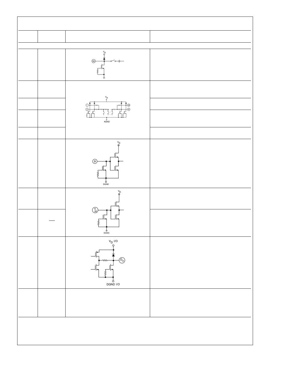
Pin Descriptions and Equivalent Circuits
Pin
No.
Symbol
Equivalent Circuit
Description
Analog I/O
30
V
IN
Analog Input signal to be converted. Conversion
range is V
REF+
S to V
REF−
S.
31
V
REF+
F
Analog input that goes to the high side of the
reference ladder of the ADC. This voltage should
force V
REF+
S to be in the range of 2.3V to 4.0V.
32
V
REF+
S
Analog output used to sense the voltage near the top
of the ADC reference ladder.
2
V
REF−
F
Analog input that goes to the low side of the
reference ladder of the ADC. This voltage should
force V
REF−
S to be in the range of 1.3V to 3.0V.
1
V
REF−
S
Analog output used to sense the voltage near the
bottom of the ADC reference ladder.
9
CLK
Converter digital clock input. V
IN
is sampled on the
falling edge of CLK input.
8
PD
Power Down input. When this pin is high, the
converter is in the Power Down mode and the data
output pins are in a high impedance state.
26
OE
Output Enable pin. When this pin and the PD pin are
low, the output data pins are active. When this pin or
the PD pin is high, the output data pins are in a high
impedance state.
14 thru
19
and
22 thru
25
D0 -D9
Digital Output pins providing the 10 bit conversion
results. D0 is the LSB, D9 is the MSB. Valid data is
present just after the falling edge of the CLK input.
3, 7, 28
V
A
Positive analog supply pins. These pins should be
connected to a clean, quiet voltage source of +5V. V
A
and V
D
should have a common supply and be
separately bypassed with 10µF to 50µF capacitors in
parallel with 0.1µF capacitors.
ADC10321
www.national.com
3