0 layout and grounding, Figure 7. an acceptable layout pattern, Applications information – Rainbow Electronics ADC10321 User Manual
Page 16
Applications Information
(Continued)
The clock line should be series terminated at the source end
in the characteristic impedance of that line. Use a series
resistor right after the source such that the source imped-
ance plus that series resistor equals the characteristic im-
pedance of the clock line. This resistor should be as close to
the source as possible, but in no case should it be further
away than
where t
r
is the rise time of the clock signal and t
PR
is the
propagation rate down the board. For a Board of FR-4
material, t
PR
is typically about 150 ps/inch.
To maintain a consistent impedance along the clock line, use
stripline or microstrip techniques (see Application Note AN-
1113) and avoid the use of through-holes in the line.
It might also be necessary to terminate the ADC end of the
clock line with a series RC to ground such that the resistor
value equals the characteristic impedance of the clock line
and the capacitor value is
where t
PR
is again the propagation rate down the clock line,
L is the length of the line in inches and Z
O
is the character-
istic impedance of the clock line.
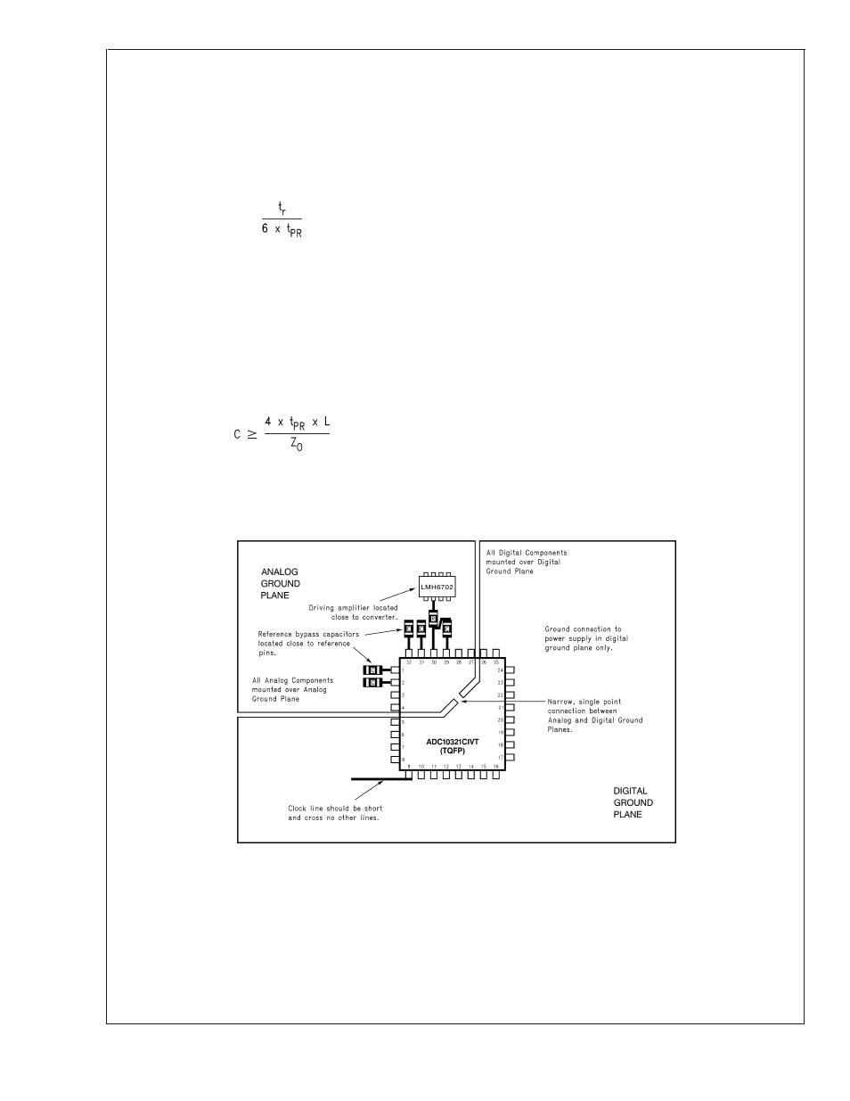
5.0 LAYOUT AND GROUNDING
Proper routing of all signals and proper ground techniques
are essential to ensure accurate conversion. Separate ana-
log and digital ground planes are required to meet data sheet
limits. The analog ground plane should be low impedance
and free of noise form other parts of the system.
Each bypass capacitor should be located as close to the
appropriate converter pin as possible and connected to the
pin and the appropriate ground plane with short traces. The
analog input should be isolated from noisy signal traces to
avoid coupling of spurious signals into the input. Any exter-
nal component (e.g., a filter capacitor) connected between
the converter’s input and ground should be connected to a
very clean point in the analog ground return.
Figure 7 gives an example of a suitable layout, including
power supply routing, ground plane separation, and bypass
capacitor placement. All analog circuitry (input amplifiers,
filters, reference components, etc.) should be placed on or
over the analog ground plane. All digital circuitry and I/O
lines should be over the digital ground plane.
Digital and analog signal lines should never run parallel to
each other in close proximity with each other. They should
only cross each other when absolutely necessary, and then
only at 90˚ angles. Violating this rule can result in digital
noise getting into the input, which degrades accuracy and
dynamic performance (THD, SNR, SINAD).
10089721
FIGURE 7. An acceptable layout pattern
ADC10321
www.national.com
16