Atr0610, Pin description, Absolute maximum ratings – Rainbow Electronics ATR0610 User Manual
Page 2: Thermal resistance, Electrical characteristics
2
ATR0610
4573C–GPS–02/03
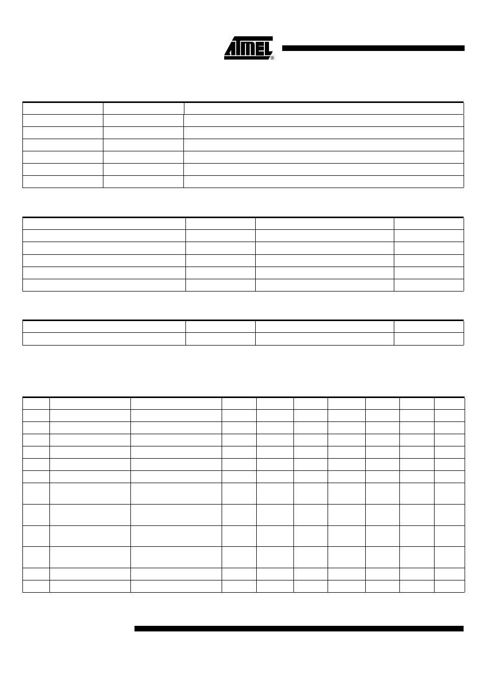
Pin Description
Pin
Symbol
Function
1
VCC
Supply voltage
2
RF_OUT
Signal output
3
DC_GND
Ground
4
RF_IN
Input for received signal
5
RF_GND
Ground for RF stage
6
PU
Power up
Absolute Maximum Ratings
Parameters
Symbol
Value
Unit
Supply voltage
V
CC
-0.3 to +3.7
V
Power-up Voltage
V
PU
-0.3 to +3.7
V
Input power
P
in
-5
dBm
Operating temperature
T
op
-40 to +85
°C
Storage temperature
T
stg
-55 to +125
°C
Thermal Resistance
Parameters
Symbol
Value
Unit
Thermal resistance
R
th
TBD
K/W
Electrical Characteristics
V
CC
= 2.7 V, V
PU
= 1.8 V, f = 1575 MHz, T
amb
= 25°C, Z
load
= 50
W
(see Figure 1)
Minimum/maximum limits are at +25°C ambient temperature, unless otherwise specified.
No.
Parameters
Test Conditions
Pin
Symbol
Min.
Typ.
Max.
Unit
Type*
1
Operating frequency
RF_IN
f
1575.42
MHz
D
2
Supply voltage
VCC
V
CC
2.7
3
3.3
V
C
3
Operating current
RF ON (V
PU
= 1.8 V)
VCC
I
3
3.3
3.5
mA
A
4
Power-down current
RF OFF(V
PU
= 0 V)
VCC
I
PD
500
nA
A
5
Small signal gain
G
15
16
17
dB
A
6
Minimum noise figure
NF
min
1.5
dB
C
7
Noise figure
Using the proposed input
matching (see Figure 1)
NF
1.6
dB
C
8
Input referred 1 dB
compression point
Caused by a DCS
blocker at 1710 MHz
Icp1
-9
dBm
A
9
Input 3
rd
-order
intercept point
f1 = 1750 MHz
f2 = 1925 MHz
IIP3
-1
dBm
C
10
Input 3
rd
-order inter-
cept point (inband)
f1 = 1575 MHz
f2 = 1577 MHz
IIP3
inb
-3
dBm
C
11
Input return loss
RL
in
10
11
dB
C
12
Output return loss
RL
out
11
12
dB
C
*) Type means: A = 100% tested, B = 100% correlation tested, C = Characterized on samples, D = Design parameter