Electrical characteristics, Ac electrical characteristics – Rainbow Electronics ADC0848 User Manual
Page 3
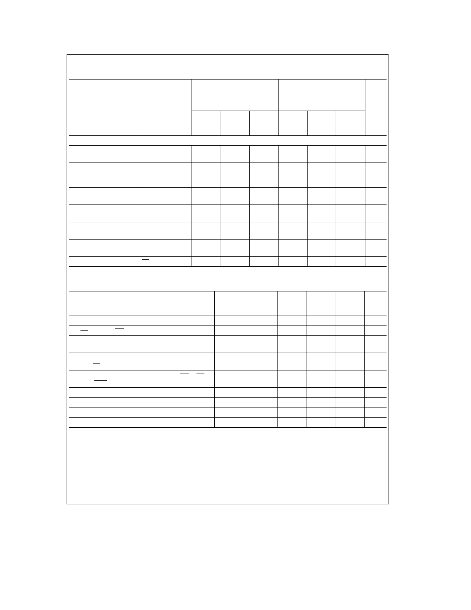
Electrical Characteristics
The following specifications apply for V
CC
e
5 V
DC
unless otherwise specified
Boldface limits apply from T
MIN
to T
MAX
all other limits T
A
e
T
j
e
25 C (Continued)
ADC0844BCJ
ADC0844BCN ADC0844CCN
ADC0844CCJ
ADC0848BCN ADC0848CCN
ADC0848BCJ
ADC0848BCV ADC0848CCV
Limit
Parameter
Conditions
ADC0848CCJ
Units
Typ
Tested
Design
Typ
Tested
Design
(Note 5)
Limit
Limit
(Note 5)
Limit
Limit
(Note 6)
(Note 7)
(Note 6)
(Note 7)
DIGITAL AND DC CHARACTERISTICS
(Continued)
I
IN(0)
Logical ‘‘0’’ Input
V
IN
e
0V
b
0 005
b
1
b
0 005
b
1
m
A
Current (Max)
V
OUT(1)
Logical ‘‘1’’
V
CC
e
4 75V
Output Voltage (Min)
I
OUT
e b
360 mA
2 4
2 8
2 4
V
I
OUT
e b
10 mA
4 5
4 6
4 5
V
V
OUT(0)
Logical ‘‘0’’
V
CC
e
4 75V
0 4
0 34
0 4
V
Output Voltage (Max)
I
OUT
e
1 6 mA
I
OUT
TRI-STATE Output
V
OUT
e
0V
b
0 01
b
3
b
0 01
b
0 3
b
3
m
A
Current (Max)
V
OUT
e
5V
0 01
3
0 01
0 3
3
m
A
I
SOURCE
Output Source
V
OUT
e
0V
b
14
b
6 5
b
14
b
7 5
b
6 5
mA
Current (Min)
I
SINK
Output Sink
V
OUT
e
V
CC
16
8 0
16
9 0
8 0
mA
Current (Min)
I
CC
Supply Current (Max)
CSe1 V
REF
Open
1
2 5
1
2 3
2 5
mA
AC Electrical Characteristics
The following specifications apply for V
CC
e
5V
DC
t
r
e
t
f
e
10 ns unless
otherwise specified Boldface limits apply from T
MIN
to T
MAX
all other limits T
A
e
T
j
e
25 C
Tested
Design
Parameter
Conditions
Typ
Limit
Limit
Units
(Note 5)
(Note 6)
(Note 7)
t
C
Maximum Conversion Time (See Graph)
30
40
60
m
s
t
W(WR)
Minimum WR Pulse Width
(Note 11)
50
150
ns
t
ACC
Maximum Access Time (Delay from Falling Edge of
C
L
e
100 pF
145
225
ns
RD to Output Data Valid)
(Note 11)
t
1H
t
0H
TRI-STATE Control (Maximum Delay from Rising
C
L
e
10 pF R
L
e
10k
125
200
ns
Edge of RD to Hi-Z State)
(Note 11)
t
WI
t
RI
Maximum Delay from Falling Edge of WR or RD to
(Note 11)
200
400
ns
Reset of INTR
t
DS
Minimum Data Set-Up Time
(Note 11)
50
100
ns
t
DH
Minimum Data Hold Time
(Note 11)
0
50
ns
C
IN
Capacitance of Logic Inputs
5
pF
C
OUT
Capacitance of Logic Outputs
5
pF
Note 1
Absolute Maximum Ratings indicate limits beyond which damage to the device may occur DC and AC electrical specifications do not apply when operating
the device beyond its specified operating conditions
Note 2
All voltages are measured with respect to the ground pins
Note 3
When the input voltage (V
IN
) at any pin exceeds the power supply rails (V
IN
k
V
b
or V
IN
l
V
a
) the absolute value of the current at that pin should be
limited to 5 mA or less The 20 mA package input current limits the number of pins that can exceed the power supply boundaries with a 5 mA current limit to four
Note 4
Human body model 100 pF discharged through a 1 5 kX resistor
Note 5
Typicals are at 25 C and represent most likely parametric norm
Note 6
Tested limits are guaranteed to National’s AOQL (Average Outgoing Quality Level)
Note 7
Design limits are guaranteed by not 100% tested These limits are not used to calculate outgoing quality levels
Note 8
Total unadjusted error includes offset full-scale linearity and multiplexer error
3