Absolute maximum ratings, Operating conditions, Electrical characteristics – Rainbow Electronics ADC0848 User Manual
Page 2
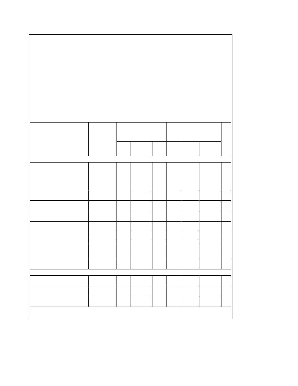
Absolute Maximum Ratings
(Notes 1
2)
If Military Aerospace specified devices are required
please contact the National Semiconductor Sales
Office Distributors for availability and specifications
Supply Voltage (V
CC
)
6 5V
Voltage
Logic Control Inputs
b
0 3V to a15V
At Other Inputs and Outputs
b
0 3V to V
CC
a
0 3V
Input Current at Any Pin (Note 3)
5 mA
Package Input Current (Note 3)
20 mA
Storage Temperature
b
65 C to a150 C
Package Dissipation at T
A
e
25 C
875 mW
ESD Susceptibility (Note 4)
800V
Lead Temperature (Soldering 10 seconds)
Dual-In-Line Package (Plastic)
260 C
Dual-In-Line Package (Ceramic)
300 C
Molded Chip Carrier Package
Vapor Phase (60 seconds)
215 C
Infrared (15 seconds)
220 C
Operating Conditions
(Notes 1
2)
Supply Voltage (V
CC
)
4 5 V
DC
to 6 0 V
DC
Temperature Range
T
MIN
s
T
A
s
T
MAX
ADC0844BCN ADC0844CCN
0 C
s
T
A
s
70 C
ADC0848BCN ADC0848CCN
ADC0844BCJ ADC0844CCJ
b
40 C
s
T
A
s
85 C
ADC0848BCJ ADC0848CCJ
ADC0848BCV ADC0848CCV
Electrical Characteristics
The following specifications apply for V
CC
e
5 V
DC
unless otherwise specified
Boldface limits apply from T
MIN
to T
MAX
all other limits T
A
e
T
j
e
25 C
ADC0844BCJ
ADC0844BCN ADC0844CCN
ADC0844CCJ
ADC0848BCN ADC0848CCN
ADC0848BCJ
ADC0848BCV ADC0848CCV
Limit
Parameter
Conditions
ADC0848CCJ
Units
Typ
Tested
Design
Typ
Tested
Design
(Note 5)
Limit
Limit
(Note 5)
Limit
Limit
(Note 6)
(Note 7)
(Note 6)
(Note 7)
CONVERTER AND MULTIPLEXER CHARACTERISTICS
Maximum Total
V
REF
e
5 00 V
DC
Unadjusted Error
(Note 8)
ADC0844BCN ADC0848BCN BCV
g
g
LSB
ADC0844BCJ ADC0848BCJ
g
LSB
ADC0844CCN ADC0848CCN CCV
g
1
g
1
LSB
ADC0844CCJ ADC0848CCJ
g
1
LSB
Minimum Reference
2 4
1 1
2 4
1 2
1 1
kX
Input Resistance
Maximum Reference
2 4
5 9
2 4
5 4
5 9
kX
Input Resistance
Maximum Common-Mode
(Note 9)
V
CC
a
0 05
V
CC
a
0 05 V
CC
a
0 05
V
Input Voltage
Minimum Common-Mode
(Note 9)
GNDb0 05
GNDb0 05 GNDb0 05
V
Input Voltage
DC Common-Mode Error
Differential Mode
g
g
g
g
g
LSB
Power Supply Sensitivity
V
CC
e
5V
g
5%
g
g
g
g
g
LSB
Off Channel Leakage
(Note 10)
Current
On Channele5V
b
1
b
0 1
b
1
m
A
Off Channele0V
On Channele0V
1
0 1
1
m
A
Off Channele5V
DIGITAL AND DC CHARACTERISTICS
V
IN(1)
Logical ‘‘1’’ Input
V
CC
e
5 25V
2 0
2 0
2 0
V
Voltage (Min)
V
IN(0)
Logical ‘‘0’’ Input
V
CC
e
4 75V
0 8
0 8
0 8
V
Voltage (Max)
I
IN(1)
Logical ‘‘1’’ Input
V
IN
e
5 0V
0 005
1
0 005
1
m
A
Current (Max)
2